ZHCSFT7 December 2016 DRV401-Q1
PRODUCTION DATA.
- 1 特性
- 2 应用
- 3 说明
- 4 修订历史记录
- 5 Pin Configuration and Functions
- 6 Specifications
-
7 Detailed Description
- 7.1 Overview
- 7.2 Functional Block Diagram
- 7.3
Feature Description
- 7.3.1 Magnetic Probe (Sensor) Interface
- 7.3.2 PWM Processing
- 7.3.3 Compensation Driver
- 7.3.4 External Compensation Coil Driver
- 7.3.5 Shunt Sense Amplifier
- 7.3.6 Over-Range Comparator
- 7.3.7 Voltage Reference
- 7.3.8 Demagnetization
- 7.3.9 Power-On and Brownout
- 7.3.10 Error Conditions
- 7.3.11 Protection Recommendations
- 7.4 Device Functional Modes
- 8 Application and Implementation
- 9 Power Supply Recommendations
- 10Layout
- 11器件和文档支持
- 12机械、封装和可订购信息
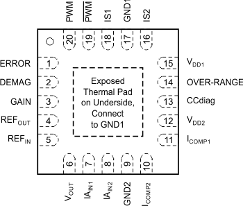
5 Pin Configuration and Functions
RGW Package
20-Pin VQFN With Exposed Thermal Pad
Top View

Pin Functions
| PIN | I/O | DESCRIPTION | |
|---|---|---|---|
| NAME | NO. | ||
| CCdiag | 13 | I | Control input for wire-break detection: high = enable |
| DEMAG | 2 | I | Control input; See the Demagnetization section. |
| ERROR | 1 | O | Error flag: open-drain output. See the Error Conditions section. |
| GAIN | 3 | I | Control input for open-loop gain: low = normal, high = −8 dB |
| GND1 | 17 | — | Ground connection |
| GND2 | 9 | — | Ground connection. Connect to GND1. |
| IAIN1 | 8 | I | Inverting input of differential amplifier |
| IAIN2 | 7 | I | Noninverting input of differential amplifier |
| ICOMP1 | 11 | O | Output 1 of compensation coil driver |
| ICOMP2 | 10 | O | Output 2 of compensation coil driver |
| IS1 | 18 | I/O | Probe connection 1 |
| IS2 | 16 | I/O | Probe connection 2 |
| OVER-RANGE | 14 | O | Open-drain output for overrange indication: low = overrange |
| PWM | 19 | O | PWM output from probe circuit (inverted) |
| PWM | 20 | O | PWM output from probe circuit |
| REFOUT | 4 | O | Output for internal 2.5-V reference voltage |
| REFIN | 5 | I | Input for zero reference to differential amplifier |
| Thermal pad | — | — | Exposed thermal pad. Connect to GND1. |
| VDD1 | 15 | — | Supply voltage |
| VDD2 | 12 | — | Supply voltage. Connect to VDD1. |
| VOUT | 6 | O | Output for differential amplifier |