ZHCS819G March   2012  – March 2018 DRV110

PRODUCTION DATA.  

  1. 特性
  2. 应用
  3. 说明
    1.     Device Images
      1.      DRV110 由电源线电压供电
  4. 修订历史记录
  5. Pin Configuration and Functions
    1.     Pin Functions
  6. Specifications
    1. 6.1 Absolute Maximum Ratings
    2. 6.2 ESD Ratings
    3. 6.3 Recommended Operating Conditions
    4. 6.4 Thermal Information
    5. 6.5 Electrical Characteristics
    6. 6.6 Typical Characteristics
  7. Detailed Description
    1. 7.1 Overview
    2. 7.2 Functional Block Diagram
    3. 7.3 Feature Description
      1. 7.3.1 Keep Time
      2. 7.3.2 PWM Current Control
      3. 7.3.3 Configuring Peak and Hold Currents
      4. 7.3.4 Configuring the PWM Frequency
      5. 7.3.5 Voltage Supply and Integrated Zener Diode
    4. 7.4 Device Functional Modes
      1. 7.4.1 Normal Mode
      2. 7.4.2 Shutdown
  8. Application and Implementation
    1. 8.1 Application Information
    2. 8.2 Typical Application
      1. 8.2.1 Design Requirements
      2. 8.2.2 Detailed Design Procedure
        1. 8.2.2.1 Current Limiting Resistor Selection
        2. 8.2.2.2 Passive Component Selection
      3. 8.2.3 Application Curve
  9. Power Supply Recommendations
  10. 10Layout
    1. 10.1 Layout Guidelines
    2. 10.2 Layout Example
  11. 11器件和文档支持
    1. 11.1 文档支持
      1. 11.1.1 相关文档
    2. 11.2 接收文档更新通知
    3. 11.3 社区资源
    4. 11.4 商标
    5. 11.5 静电放电警告
    6. 11.6 Glossary
  12. 12机械、封装和可订购信息

封装选项

机械数据 (封装 | 引脚)
散热焊盘机械数据 (封装 | 引脚)
订购信息

PWM Current Control

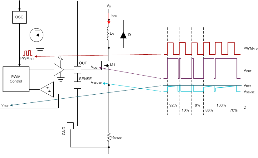
The current control loop regulates, cycle-by-cycle, the solenoid current by sensing voltage at the SENSE pin and controlling the external switching device gate through the OUT pin. During the ON-cycle, the OUT pin voltage is driven and kept high (equal to VIN voltage) allowing current to flow through the external switch as long as the voltage at the SENSE pin is less than VREF. As soon as the voltage at the SENSE pin is above VREF, the OUT pin voltage is immediately driven low and kept low until the next ON-cycle is triggered by the internal PWM clock signal. In the beginning of each ON-cycle, the OUT pin voltage is driven high and kept high for at least the time determined by the minimum PWM signal duty cycle, DMIN.

Because the current sense is done by comparing the voltage at the SENSE pin to a reference voltage, the DRV110 device acts like a hysteresis controller. When the device acts like a hysteresis controller, it can make the PWM frequency and duty cycle appear uneven for some solenoids (see Figure 3).
DRV110 drv110-current-control-with-varying-out-duty-cycle.gif
The DRV110 device measures the voltage at the SENSE node (VSENSE). This voltage is compared against the reference voltage (VREF) each clock cycle. The voltage at the output node (VOUT) becomes low when VSENSE ≥ VREF. The duty cycle (D) of the output voltage varies from 8% to 100%. In summary, the SENSE voltage is sampled after each rising edge of the PWM CLK signal (PWMCLK) and goes low when VSENSE ≥ VREF at a minimum duty cycle of 8%.
Figure 3. DRV110 Current Control with Varying OUT Duty Cycle