ZHCSEQ8 March   2016 DRV10964

PRODUCTION DATA.  

  1. 特性
  2. 应用范围
  3. 说明
  4. 修订历史记录
  5. Pin Configuration and Functions
  6. Specifications
    1. 6.1 Absolute Maximum Ratings
    2. 6.2 ESD Ratings
    3. 6.3 Recommended Operating Conditions
    4. 6.4 Thermal Information
    5. 6.5 Electrical Characteristics
    6. 6.6 Typical Characteristics
  7. Detailed Description
    1. 7.1 Overview
    2. 7.2 Functional Block Diagram
    3. 7.3 Feature Description
      1. 7.3.1  Sleep Mode
      2. 7.3.2  Speed Input and Control
      3. 7.3.3  Motor Direction Change
      4. 7.3.4  Motor Frequency Feedback (FG)
        1. 7.3.4.1 Tach Feedback During Spin Down
      5. 7.3.5  Lock Detection
        1. 7.3.5.1 Lock0: No Motor
        2. 7.3.5.2 Lock1: Frequency Overflow
        3. 7.3.5.3 Lock2: BEMF Abnormal
          1. 7.3.5.3.1 Lock 3: Accelerate Abnormal
        4. 7.3.5.4 Lock4: Speed Abnormal
      6. 7.3.6  Short Circuit Current Protection
      7. 7.3.7  Anti-Voltage Surge (AVS)
        1. 7.3.7.1 Protecting Against the Return of Mechanical Energy
        2. 7.3.7.2 Protecting Against the Return of Inductive Energy
      8. 7.3.8  Overtemperature Protection
      9. 7.3.9  Undervoltage Protection
      10. 7.3.10 CONFIG Configuration
    4. 7.4 Device Functional Modes
      1. 7.4.1 Spin up Settings
        1. 7.4.1.1 Motor Kt and Rm
        2. 7.4.1.2 Motor Start
        3. 7.4.1.3 Initial Speed Detect (ISD)
        4. 7.4.1.4 Align
        5. 7.4.1.5 Handoff and Closed Loop
  8. Application and Implementation
    1. 8.1 Application Information
    2. 8.2 Typical Application
      1. 8.2.1 Design Requirements
      2. 8.2.2 Detailed Design Procedure
      3. 8.2.3 Application Curves
  9. Power Supply Recommendations
  10. 10Layout
    1. 10.1 Layout Guidelines
    2. 10.2 Layout Example
  11. 11器件和文档支持
    1. 11.1 社区资源
    2. 11.2 商标
    3. 11.3 静电放电警告
    4. 11.4 Glossary
  12. 12机械、封装和可订购信息

封装选项

机械数据 (封装 | 引脚)
散热焊盘机械数据 (封装 | 引脚)
订购信息

10 Layout

10.1 Layout Guidelines

The package uses an exposed pad to remove heat from the device. For proper operation, this pad must be thermally connected to copper on the PCB to dissipate heat. On a multi-layer PCB with a ground plane, this can be accomplished by adding a number of vias to connect the thermal pad to the ground plane. On PCBs without internal planes, copper area can be added on either side of the PCB to dissipate heat. If the copper area is on the opposite side of the PCB from the device, thermal vias are used to transfer the heat between top and bottom layers.

For details about how to design the PCB, refer to TI application report, PowerPAD™ Thermally Enhanced Package (SLMA002), and TI application brief, PowerPAD™ Made Easy (SLMA004), available at www.ti.com. In general, the more copper area that can be provided, the more power can be dissipated.

10.2 Layout Example
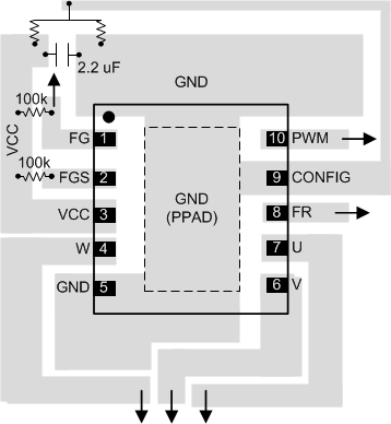
DRV10964 layout_example_01_slas955.gif Figure 21. DRV10964 Layout Example