ZHCSD23A October 2014 – February 2016 DLP6500FYE
PRODUCTION DATA.
- 1 特性
- 2 应用
- 3 说明
- 4 修订历史记录
- 5 Pin Configuration and Functions
-
6 Specifications
- 6.1 Absolute Maximum Ratings
- 6.2 Storage Conditions
- 6.3 ESD Ratings
- 6.4 Recommended Operating Conditions
- 6.5 Thermal Information
- 6.6 Electrical Characteristics
- 6.7 Timing Requirements
- 6.8 Typical Characteristics
- 6.9 System Mounting Interface Loads
- 6.10 Micromirror Array Physical Characteristics
- 6.11 Micromirror Array Optical Characteristics
- 6.12 Window Characteristics
- 6.13 Chipset Component Usage Specification
- 7 Detailed Description
- 8 Application and Implementation
- 9 Power Supply Recommendations
- 10Layout
- 11器件文档支持
- 12机械、封装和可订购信息
6 Specifications
6.1 Absolute Maximum Ratings
over operating free-air temperature range (unless otherwise noted) (1)| SUPPLY VOLTAGES | MIN | MAX | UNIT | |
| VCC | Supply voltage for LVCMOS core logic (2) | –0.5 | 4 | V |
| VCCI | Supply voltage for LVDS receivers (2) | –0.5 | 4 | V |
| VOFFSET | Supply voltage for HVCMOS and micromirror electrode (2) (3) | –0.5 | 9 | V |
| VBIAS | Supply voltage for micromirror electrode (2) | –0.5 | 17 | V |
| VRESET | Supply voltage for micromirror electrode (2) | –11 | 0.5 | V |
| | VCC – VCCI | | Supply voltage delta (absolute value) (4) | 0.3 | V | |
| | VBIAS – VOFFSET | | Supply voltage delta (absolute value) (5) | 8.75 | V | |
| INPUT VOLTAGES | ||||
| Input voltage for all other LVCMOS input pins (2) | –0.5 | VCC + 0.15 | V | |
| Input voltage for all other LVDS input pins (2) (6) | –0.5 | VCCI + 0.15 | V | |
| | VID | | Input differential voltage (absolute value) (7) | 700 | mV | |
| IID | Input differential current (7) | 7 | mA | |
| CLOCKS | ||||
| ƒclock | Clock frequency for LVDS interface, DCLK (all channels) | 460 | MHz | |
| ENVIRONMENTAL | ||||
| TCASE | Case temperature: operational (8) (9) | –20 | 90 | ºC |
| Case temperature: non–operational (9) | –40 | 90 | ºC | |
| Dew Point (Operating and non-Operating) | 81 | ºC | ||
6.2 Storage Conditions
applicable before the DMD is installed in the final product| MIN | MAX | UNIT | ||
|---|---|---|---|---|
| Tstg | DMD Storage Temperature | –40 | 85 | °C |
| TDP | Storage Dew Point - long-term (1) | 24 | °C | |
| Storage Dew Point - short-term (2) | 28 | °C |
6.3 ESD Ratings
| VALUE | UNIT | |||
|---|---|---|---|---|
| V(ESD) | Electrostatic discharge | Human-body model (HBM), per ANSI/ESDA/JEDEC JS-001(1) | ±2000 | V |
6.4 Recommended Operating Conditions
over operating free-air temperature range (unless otherwise noted)| MIN | NOM | MAX | UNIT | ||
|---|---|---|---|---|---|
| SUPPLY VOLTAGES(1) (2) | |||||
| VCC | Supply voltage for LVCMOS core logic | 3.15 | 3.3 | 3.45 | V |
| VCCI | Supply voltage for LVDS receivers | 3.15 | 3.3 | 3.45 | V |
| VOFFSET | Supply voltage for HVCMOS and micromirror electrodes(2) | 8.25 | 8.5 | 8.75 | V |
| VBIAS | Supply voltage for micromirror electrodes | 15.5 | 16 | 16.5 | V |
| VRESET | Supply voltage for micromirror electrodes | –9.5 | –10 | –10.5 | V |
| |VCCI–VCC| | Supply voltage delta (absolute value) (3) | 0.3 | V | ||
| |VBIAS–VOFFSET| | Supply voltage delta (absolute value)(4) | 8.75 | V | ||
| LVCMOS PINS | |||||
| VIH | High level Input voltage (5) | 1.7 | 2.5 | VCC + 0.15 | V |
| VIL | Low level Input voltage(5) | – 0.3 | 0.7 | V | |
| IOH | High level output current at VOH = 2.4 V | –20 | mA | ||
| IOL | Low level output current at VOL = 0.4 V | 15 | mA | ||
| TPWRDNZ | PWRDNZ pulse width(6) | 10 | ns | ||
| SCP INTERFACE(7) | |||||
| ƒclock | SCP clock frequency(8) | 500 | kHz | ||
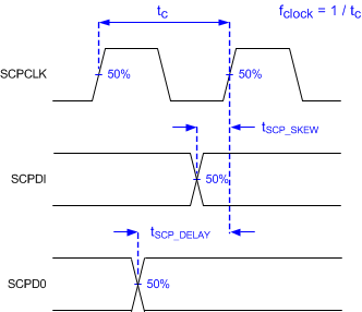
| tSCP_SKEW | Time between valid SCPDI and rising edge of SCPCLK(9) | –800 | 800 | ns | |
| tSCP_DELAY | Time between valid SCPDO and rising edge of SCPCLK(9) | 700 | ns | ||
| tSCP_BYTE_INTERVAL | Time between consecutive bytes | 1 | µs | ||
| tSCP_NEG_ENZ | Time between falling edge of SCPENZ and the first rising edge of SCPCLK | 30 | ns | ||
| tSCP_PW_ENZ | SCPENZ inactive pulse width (high level) | 1 | µs | ||
| tSCP_OUT_EN | Time required for SCP output buffer to recover after SCPENZ (from tri-state) | 1.5 | ns | ||
| ƒclock | SCP circuit clock oscillator frequency (10) | 9.6 | 11.1 | MHz | |
| LVDS INTERFACE | |||||
| ƒclock | Clock frequency for LVDS interface, DCLK (all channels) | 400 | MHz | ||
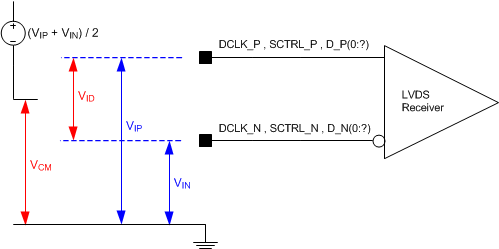
| |VID| | Input differential voltage (absolute value)(11) | 100 | 400 | 600 | mV |
| VCM | Common mode (11) | 1200 | mV | ||
| VLVDS | LVDS voltage(11) | 0 | 2000 | mV | |
| tLVDS_RSTZ | Time required for LVDS receivers to recover from PWRDNZ | 10 | ns | ||
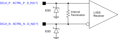
| ZIN | Internal differential termination resistance | 95 | 105 | Ω | |
| ZLINE | Line differential impedance (PWB/trace) | 90 | 100 | 110 | Ω |
| ENVIRONMENTAL (12) | |||||
| TDMD | DMD temperature–operational, long-term (13) (14) (18) | 0 | 40 to 70(14) | °C | |
| DMD temperature – operational, short-term | –20 | 75 | °C | ||
| TWINDOW | Window temperature – operational(15) | 90 | °C | ||
| TCERAMIC-WINDOW-DELTA | Delta ceramic-to-window temperature -operational (15) (16) | 30 | °C | ||
| Long-term dew point (operational, non-operational, long-term) | 24 | °C | |||
| Short-term dew point(18) (19) (operational, non-operational, short-term) | 28 | °C | |||
| ILLUV | Illumination, wavelength < 420 nm | 0.68 | mW/cm2 | ||
| ILLVIS | Illumination, wavelengths between 420 and 700 nm | Thermally Limited(17) | mW/cm2 | ||
| ILLIR | Illumination, wavelength > 700 nm | 10 | mW/cm2 | ||
Frequency = 60MHz. Maximum Rise Time = 2.5 ns at (20% to 80%)
Frequency = 60MHz. Maximum Fall Time = 2.5 ns at (80% to 20%)
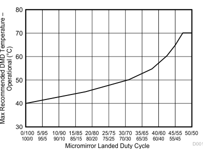 Figure 1. Max Recommended DMD Temperature – Derating Curve
6.5 Thermal Information
| THERMAL METRIC(1) | DLP6500FYE | UNIT | |||
|---|---|---|---|---|---|
| MIN | FYE (350) | MAX | |||
| Active Area-to-Case Ceramic Thermal resistance (1) | 0.6 | °C/W | |||
6.6 Electrical Characteristics
over operating free-air temperature range (unless otherwise noted)| PARAMETER | DESCRIPTION | TEST CONDITIONS(1) | MIN | TYP | MAX | UNIT |
|---|---|---|---|---|---|---|
| VOH | High-level output voltage | VCC = 3.3 V, IOH = –20 mA | 2.4 | V | ||
| VOL | Low level output voltage | VCC = 3.45 V, IOL = 15 mA | 0.4 | V | ||
| IIH | High–level input current(2) (3) | VCC = 3.45 V , VI = VCC | 250 | µA | ||
| IlL | Low level input current | VCC = 3.45 V, VI = 0 | –250 | µA | ||
| IOZ | High–impedance output current | VCC = 3.45 V | 10 | µA | ||
| CURRENT | ||||||
| ICC | Supply current (4) | VCC = 3.6 V | 1076 | mA | ||
| ICCI | VCCI = 3.6 V | 518 | ||||
| IOFFSET | Supply current (5) | VOFFSET = 8.75 V | 4 | mA | ||
| IBIAS | VBIAS = 16.5 V | 14 | ||||
| IRESET | Supply current | VRESET = –10.5 V | 11 | mA | ||
| ITOTAL | Total Sum | 1623 | ||||
| POWER | ||||||
| PCC | Supply power dissipation | VCC = 3.6 V | 3874 | mW | ||
| PCCI | VCCI = 3.6 V | 1865 | ||||
| POFFSET | VOFFSET = 8.75 V | 35 | ||||
| PBIAS | VBIAS = 16.5 V | 231 | ||||
| PRESET | VRESET = –10.5 V | 116 | ||||
| PTOTAL | Supply power dissipation(6) | Total Sum | 6300 | |||
| CAPACITANCE | ||||||
| CI | Input capacitance | ƒ = 1 MHz | 10 | pF | ||
| CO | Output capacitance | ƒ = 1 MHz | 10 | pF | ||
| CM | Reset group capacitance MBRST(14:0) | ƒ = 1 MHz 1920 × 72 micromirrors | 330 | 390 | pF | |
6.7 Timing Requirements
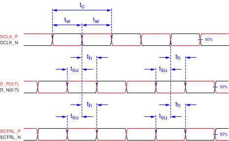
Over Recommended Operating Conditions unless otherwise noted.| DESCRIPTION(1) | MIN | TYP | MAX | UNIT | |||
|---|---|---|---|---|---|---|---|
| SCP INTERFACE(2) | |||||||
| tr | Rise time | 20% to 80% | 200 | ns | |||
| tƒ | Fall time | 80% to 20% | 200 | ns | |||
| LVDS INTERFACE(2) | |||||||
| tr | Rise time | 20% to 80% | 100 | 400 | ps | ||
| tƒ | Fall time | 80% to 20% | 100 | 400 | ps | ||
| LVDS CLOCKS(3) | |||||||
| tc | Cycle time | DCLK_A, 50% to 50% | 2.5 | ns | |||
| DCLK_B, 50% to 50% | 2.5 | ||||||
| tw | Pulse duration | DCLK_A, 50% to 50% | 1.19 | 1.25 | ns | ||
| DCLK_B, 50% to 50% | 1.19 | 1.25 | |||||
| LVDS INTERFACE(3) | |||||||
| tsu | Setup time | D_A(15:0) before rising or falling edge of DCLK_A | 0.1 | ns | |||
| D_B(15:0) before rising or falling edge of DCLK_B | 0.1 | ||||||
| tsu | Setup time | SCTRL_A before rising or falling edge of DCLK_A | 0.1 | ns | |||
| SCTRL_B before rising or falling edge of DCLK_B | 0.1 | ||||||
| th | Hold time | D_A(15:0) after rising or falling edge of DCLK_A | 0.4 | ns | |||
| D_B(15:0) after rising or falling edge of DCLK_B | 0.4 | ||||||
| th | Hold time | SCTRL_A after rising or falling edge of DCLK_A | 0.3 | ns | |||
| SCTRL_B after rising or falling edge of DCLK_B | 0.3 | ||||||
| LVDS INTERFACE(4) | |||||||
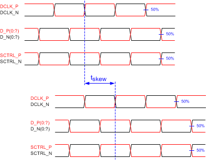
| tskew | Skew time | Channel B relative to Channel A (4) | Channel A includes the following LVDS pairs: DCLK_AP and DCLK_AN SCTRL_AP and SCTRL_AN D_AP(15:0) and D_AN(15:0) |
–1.25 | 1.25 | ns | |
| Channel B includes the following LVDS pairs: DCLK_BP and DCLK_BN SCTRL_BP and SCTRL_BN D_BP(15:0) and D_BN(15:0) |
|||||||
Timing Requirements
The data sheet provides timing at the device pin. For output timing analysis, the tester pin electronics and its transmission line effects must be taken into account. Figure 2 shows an equivalent test load circuit for the output under test. The load capacitance value stated is only for characterization and measurement of AC timing signals. This load capacitance value does not indicate the maximum load the device is capable of driving.
Timing reference loads are not intended as a precise representation of any particular system environment or depiction of the actual load presented by a production test. System designers should use IBIS or other simulation tools to correlate the timing reference load to a system environment. Refer to the Application and Implementation section.
 Figure 2. Test Load Circuit


6.8 Typical Characteristics
The DLP6500FYE DMD is controlled by the DLPC900 controller. The controller has two modes of operation. The first is Video mode where the video source is displayed on the DMD. The second is Pattern mode, where the patterns are pre-stored in flash memory and then streamed to the DMD. The allowed DMD pattern rate depends on which mode and bit-depth is selected.Table 1. Bit Depth versus Pattern Rate
| BIT DEPTH | VIDEO MODE RATE (Hz) | PATTERN MODE RATE (Hz) |
|---|---|---|
| 1 | 2880 | 9523 |
| 2 | 1440 | 3289 |
| 3 | 960 | 2638 |
| 4 | 720 | 1364 |
| 5 | 480 | 823 |
| 6 | 480 | 672 |
| 7 | 360 | 500 |
| 8 | 247 | 247 |
6.9 System Mounting Interface Loads
| PARAMETER | MIN | NOM | MAX | UNIT | ||
|---|---|---|---|---|---|---|
Maximum system mounting interface load to be applied to the:
|
(See Figure 10) | 11.30 | Kg | |||
| Maximum Load 22.64 Applied per condition 2 | ||||||
|
(See Figure 10) | 0 | Kg | |||
| 22.60 | ||||||
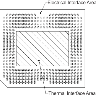 Figure 10. System Mounting Interface Loads
6.10 Micromirror Array Physical Characteristics
| VALUE | UNIT | ||||
|---|---|---|---|---|---|
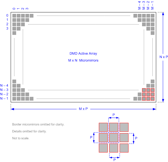
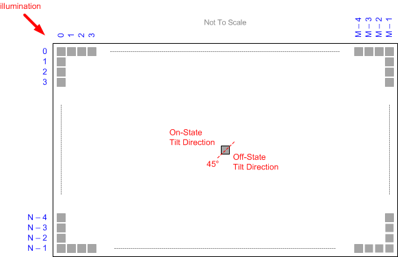
| M | Number of active columns | See Figure 11 | 1920 | micromirrors | |
| N | Number of active rows | 1080 | micromirrors | ||
| P | Micromirror (pixel) pitch | 7.56 | µm | ||
| Micromirror active array width | M × P | 14.5152 | mm | ||
| Micromirror active array height | N × P | 8.1648 | mm | ||
| Micromirror active border | Pond of micromirror (POM)(1) | 14 | micromirrors /side | ||
6.11 Micromirror Array Optical Characteristics
See Optical Interface and System Image Quality for important information
| PARAMETER | CONDITIONS | MIN | NOM | MAX | UNIT | |
|---|---|---|---|---|---|---|
| α | Micromirror tilt angle | DMD landed state (1) | 12 | ° | ||
| β | Micromirror tilt angle tolerance(1) (2) (3) (4) (5) | –1 | 1 | ° | ||
| Micromirror tilt direction(5) (6) (7) | 44 | 45 | 46 | ° | ||
| Number of out-of-specification micromirrors (8) | Adjacent micromirrors | 0 | micromirrors | |||
| Non-adjacent micromirrors | 10 | |||||
| Micromirror crossover time (9) (10) | Typical performance | 2.5 | μs | |||
| Micromirror switching time (10) | Typical performance | 5 | μs | |||
| DMD photopic efficiency within the wavelength range 420 nm to 700 nm (11) | 66% | |||||
6.12 Window Characteristics
| PARAMETER(1) | CONDITIONS | MIN | NOM | MAX | UNIT |
|---|---|---|---|---|---|
| Window material designation S600 | Corning Eagle XG | ||||
| Window refractive index | at wavelength 546.1 nm | 1.5119 | |||
| Window aperture | See (2) | ||||
| Illumination overfill | Refer to Illumination Overfill | ||||
| Window transmittance, single–pass through both surfaces and glass (3) | Minimum within the wavelength range 420 nm to 680 nm. Applies to all angles 0° to 30° AOI. | 97% | |||
| Average over the wavelength range 420 nm to 680 nm. Applies to all angles 30° to 45° AOI. | 97% |
6.13 Chipset Component Usage Specification
The DLP6500FYE is a component of one or more DLP® chipsets. Reliable function and operation of the DLP6500FYE requires that it be used in conjunction with the other components of the applicable DLP chipset, including those components that contain or implement TI DMD control technology. TI DMD control technology is the TI technology and devices for operating or controlling a DLP DMD.