ZHCSO64B September 2020 – April 2022 DLP471TE
PRODUCTION DATA
- 1 特性
- 2 应用
- 3 说明
- 4 Revision History
- 5 Pin Configuration and Functions
-
6 Specifications
- 6.1 Absolute Maximum Ratings
- 6.2 Storage Conditions
- 6.3 ESD Ratings
- 6.4 Recommended Operating Conditions
- 6.5 Thermal Information
- 6.6 Electrical Characteristics
- 6.7 Switching Characteristics
- 6.8 Timing Requirements
- 6.9 System Mounting Interface Loads
- 6.10 Micromirror Array Physical Characteristics
- 6.11 Micromirror Array Optical Characteristics
- 6.12 Window Characteristics
- 6.13 Chipset Component Usage Specification
- 7 Detailed Description
- 8 Application and Implementation
- 9 Power Supply Recommendations
- 10Layout
- 11Device and Documentation Support
- 12Mechanical, Packaging, and Orderable Information
6.10 Micromirror Array Physical Characteristics
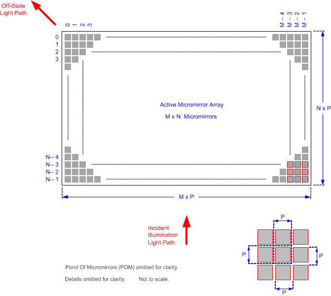
| PARAMETER DESCRIPTION | VALUE | UNIT | |
|---|---|---|---|
| Number of active columns(1)(2) | M | 1920 | micromirrors |
| Number of active rows(1)(2) | N | 1080 | micromirrors |
| Micromirror (pixel) pitch (1) | P | 5.4 | μm |
| Micromirror active array width(1) | Micromirror pitch × number of active columns | 10.368 | mm |
| Micromirror active array height(1) | Micromirror pitch × number of active rows | 5.832 | mm |
| Micromirror active border(3) | Pond of micromirror (POM) | 20 | micromirrors/side |
(1) See Figure 6-14.
(2) The fast switching speed of the DMD micromirrors combined with advanced DLP
image processing algorithms enables each micromirror to display four distinct
pixels on the screen during every frame, resulting in a full 3840 × 2160 pixel
image being displayed.
(3) The structure and qualities of the border around the active array includes a
band of partially functional micromirrors referred to as the Pond Of
Micromirrors (POM). These micromirrors are structurally and/or
electrically prevented from tilting toward the bright or ON state but still
require an electrical bias to tilt toward the OFF state.
 Figure 6-14 Micromirror Array Physical
Characteristics