ZHCSJA4B January 2019 – May 2022 DLP4500
PRODUCTION DATA
- 1 特性
- 2 应用
- 3 说明
- 4 Revision History
- 5 Chipset Component Usage Specification
- 6 Pin Configuration and Functions
-
7 Specifications
- 7.1 Absolute Maximum Ratings
- 7.2 Storage Conditions
- 7.3 ESD Ratings
- 7.4 Recommended Operating Conditions
- 7.5 Thermal Information
- 7.6 Electrical Characteristics
- 7.7 Timing Requirements
- 7.8 System Mounting Interface Loads
- 7.9 Micromirror Array Physical Characteristics
- 7.10 Micromirror Array Optical Characteristics
- 7.11 Typical Characteristics
- 8 Detailed Description
- 9 Application and Implementation
- 10Power Supply Recommendations
-
11Layout
- 11.1 Layout Guidelines
- 11.2 Layout Example
- 12Device and Documentation Support
- 13Mechanical, Packaging, and Orderable Information
7.4 Recommended Operating Conditions
over operating free-air temperature range (unless otherwise noted)
| MIN | NOM | MAX | UNIT | ||||
|---|---|---|---|---|---|---|---|
| SUPPLY VOLTAGES (1) | |||||||
| VCC | Supply voltage for LVCMOS core logic | 2.375 | 2.5 | 2.625 | V | ||
| VREF | Supply voltage for LVCMOS DDR interface | 1.6 | 1.9 | 2 | V | ||
| VOFFSET | Supply voltage for HVCMOS and micromirror electrode (3) (2) | 8.25 | 8.5 | 8.75 | V | ||
| VBIAS | Supply voltage for micromirror electrode (3) | 15.5 | 16 | 16.5 | V | ||
| VRESET | Supply voltage for micromirror electrode | –9.5 | –10 | –10.5 | V | ||
| |VBIAS – VOFFSET| | Supply voltage delta (absolute value) (3) | 8.75 | V | ||||
| VOLTAGE RANGE | |||||||
| VT+ | Positive-going threshold voltage | 0.4 × VREF | 0.7 × VREF | V | |||
| VT– | Negative-going threshold voltage | 0.3 × VREF | 0.6 × VREF | V | |||
| Vhys | Hysteresis voltage (VT+ – VT–) | 0.1 × VREF | 0.4 × VREF | V | |||
| CLOCK FREQUENCY | |||||||
| ƒ(CLK) | DCLK clock frequency | 80 | 120 | MHz | |||
| ENVIRONMENTAL (4) | |||||||
| TDMD | DMD temperature - operational, long-term (5) (7) | 10 | 40 to 70 (6) | °C | |||
| DMD temperature - operational, short-term | –20 | 70 | °C | ||||
| TWindow | DMD window temperature - operational | 0 | 90 | °C | |||
| TCERAMIC-WINDOW-DELTA | DMD |ceramic TP1 - window| temperature delta - operational (8) (10) | 0 | 15 | °C | |||
| DMD long-term dewpoint (operational, non-operational) | 24 | °C | |||||
| DMD short-term dewpoint (operational, non-operational) (9) | 28 | °C | |||||
| ILLUMINATION | |||||||
| ILLUV-VIS | Illumination power - spectral region <420 nm | 0.68 | mW/cm2 | ||||
| ILLVIS | Illumination power - spectral region 420 to 700 nm, FQE package | Thermally Limited (11) | mW/cm2 | ||||
| Illumination power - spectral region 420 to 700 nm, FQD package | Thermally Limited (11) | mW/cm2 | |||||
| ILLIR | Illumination power - spectral region >700 nm | 10 | mW/cm2 | ||||
(1) Supply voltages VCC, VREF, VOFFSET, VBIAS, and VRESET are all
required for proper DMD operation. All voltage values are referenced to common
ground VSS.
(2) VOFFSET supply transients must fall within specified max
voltages.
(3) To prevent excess current, the supply voltage delta |VBIAS –
VOFFSET| must be less than specified limit.
(4) Optimal long-term performance and optical efficiency of the
digital micromirror device (DMD) can be affected by various application
parameters, including illumination spectrum, illumination power density,
micromirror landed duty cycle, ambient temperature (storage and operating), DMD
temperature, ambient humidy (storage and operating), and power on or off duty
cycle.
(5) DMD temperature is the worst-case of any test point shown in
Figure 8-3 or Figure 8-4, or the active array as calculated by the Micromirror Array
Temperature Calculation, or any point along the window edge
as defined in Figure 8-3 or Figure 8-4. The locations of thermal test point TP2 in Figure 8-3 or Figure 8-4 is intended to measure the highest window edge temperature. If a particular
application causes another point on the window edge to be at a higher
temperature, a test point should be added to that location.
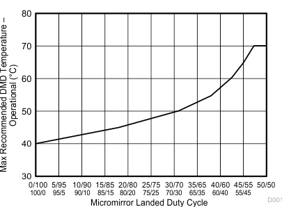
(6) Per Figure 7-1, the
maximum operational case temperature at test points TP1 and TP2 as shown in
Figure 8-3 or Figure 8-4 should be derated based on the micromirror landed duty cycle that the DMD
experiences in the end application. Refer to Micromirror
Landed-on/Landed-Off Duty Cycle for a definition of landed
duty cycle.
(7) Long-term is defined as the average over the usable life.
(8) Ceramic package and window temperature as measured at test
points TP1 and TP2 in Figure 8-3 or Figure 8-4.
(9) Dew points beyond the specified long-term dew point
(operating, non-operating, or storage) are for short-term conditions only, where
short-term is defined as <60 cumulative days over the useful life of the
device.
(10) Between any two points on or within the package including the
mirror array.
(11) Refer to Micromirror Array
Temperature Calculation and Temperature
Calculation for information related to calculating the
micromirror array temperature.
 Figure 7-1 Maximum Recommended DMD
Temperature – Derating Curve