SBAS368D May 2006 – December 2016 DDC264
PRODUCTION DATA.
- 1 Features
- 2 Applications
- 3 Description
- 4 Revision History
- 5 Device Comparison Table
- 6 Pin Configuration and Functions
- 7 Specifications
-
8 Detailed Description
- 8.1 Overview
- 8.2 Functional Block Diagram
- 8.3
Feature Description
- 8.3.1 Dual Switched Integrator: Basic Integration Cycle
- 8.3.2 Integration Capacitors
- 8.3.3 Voltage Reference
- 8.3.4 Serial Data Output and Control Interface
- 8.4 Device Functional Modes
- 8.5 Programming
- 8.6 Register Maps
- 9 Application and Implementation
- 10Power Supply Recommendations
- 11Layout
- 12Device and Documentation Support
- 13Mechanical, Packaging, and Orderable Information
7 Specifications
7.1 Absolute Maximum Ratings
over operating free-air temperature range (unless otherwise noted) (1)| MIN | MAX | UNIT | ||
|---|---|---|---|---|
| AVDD to AGND | –0.3 | 6 | V | |
| DVDD to DGND | –0.3 | 3.6 | V | |
| AGND to DGND | ±0.2 | V | ||
| VREF input to AGND | 2 | AVDD + 0.3 | V | |
| Analog input to AGND | –0.3 | 0.7 | V | |
| Digital input voltage to DGND | –0.3 | 0.3 | V | |
| Digital output voltage to DGND | –0.3 | 0.3 | V | |
| Operating temperature | 0 | 70 | °C | |
| Junction temperature, TJ | 150 | °C | ||
| Storage temperature, Tstg | –60 | 150 | °C | |
(1) Stresses beyond those listed under Absolute Maximum Ratings may cause permanent damage to the device. These are stress ratings only, which do not imply functional operation of the device at these or any other conditions beyond those indicated under Recommended Operating Conditions. Exposure to absolute-maximum-rated conditions for extended periods may affect device reliability.
7.2 ESD Ratings
| VALUE | UNIT | ||||
|---|---|---|---|---|---|
| V(ESD) | Electrostatic discharge | Human body model (HBM), per ANSI/ESDA/JEDEC JS-001, all pins(1) | ±4000 | V | |
| Charged device model (CDM), per JEDEC specification JESD22-C101, all pins(2) | ±1000 | ||||
(1) JEDEC document JEP155 states that 500-V HBM allows safe manufacturing with a standard ESD control process.
(2) JEDEC document JEP157 states that 250-V CDM allows safe manufacturing with a standard ESD control process.
7.3 Recommended Operating Conditions
over operating free-air temperature range (unless otherwise noted)| MIN | NOM | MAX | UNIT | ||||
|---|---|---|---|---|---|---|---|
| VREF | Reference voltage | 4 | 4.096 | 4.2 | V | ||
| POWER-SUPPLY REQUIREMENTS | |||||||
| Analog power supply voltage (AVDD) | DDC264C | 4.75 | 5 | 5.25 | V | ||
| DDC264CK | 4.9 | 5 | 5.1 | ||||
| Digital power supply voltage (DVDD) | 2.7 | 3.3 | 3.6 | V | |||
| DYNAMIC CHARACTERISTICS | |||||||
| Data rate | DDC264C | 3 | 3.125 | kSPS | |||
| DDC264CK | 6 | 6.25 | |||||
| tINT | Integration time | DDC264C | 320 | 333 | 1,000,000 | µs | |
| DDC264CK | 160 | 166 | 1,000,000 | ||||
| System clock | Clkdiv = 0 | DDC264C | 1 | 5 | MHz | ||
| DDC264CK | 1 | 10 | |||||
| Clkdiv = 1 | DDC264C | 4 | 20 | MHz | |||
| DDC264CK | 4 | 40 | |||||
| Data clock (DCLK) | 32 | MHz | |||||
| Configuration clock (CLK_CFG) | 20 | MHz | |||||
7.4 Thermal Information
| THERMAL METRIC(1) | DDC264C, DDC264CK |
UNIT | |
|---|---|---|---|
| ZAW (NFBGA) | |||
| 100 PINS | |||
| RθJA | Junction-to-ambient thermal resistance | 25.7 | °C/W |
| RθJC(top) | Junction-to-case (top) thermal resistance | 9.8 | °C/W |
| RθJB | Junction-to-board thermal resistance | 7.1 | °C/W |
| ψJT | Junction-to-top characterization parameter | 0.1 | °C/W |
| ψJB | Junction-to-board characterization parameter | 7 | °C/W |
| RθJC(bot) | Junction-to-case (bottom) thermal resistance | — | °C/W |
(1) For more information about traditional and new thermal metrics, see the Semiconductor and IC Package Thermal Metrics application report.
7.5 Electrical Characteristics
at TA = 25°C, AVDD = 5 V, DVDD = 3 V, VREF = 4.096 V, tINT = 333 µs for DDC264C or 166 µs for DDC264CK,and range = 3 (150 pC) (unless otherwise noted)
| PARAMETER | TEST CONDITIONS | MIN | TYP | MAX | UNIT | ||
|---|---|---|---|---|---|---|---|
| ANALOG INPUT | |||||||
| Range 0 | 10.5 | 12.5 | 14.5 | pC | |||
| Range 1 | 47.5 | 50 | 52.5 | pC | |||
| Range 2 | 95 | 100 | 105 | pC | |||
| Range 3 | 142.5 | 150 | 157.5 | pC | |||
| Negative full-scale range | –0.4% of Positive full-scale range | pC | |||||
| ACCURACY | |||||||
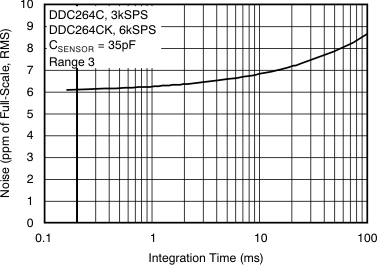
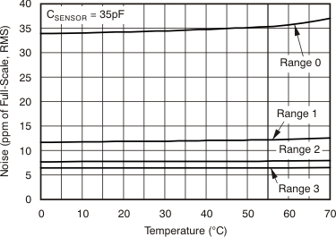
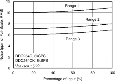
| Noise, low-level input(1) | Range = 3, CSENSOR(2) = 35 pF | 6.3 | ppm of FSR(3), rms | ||||
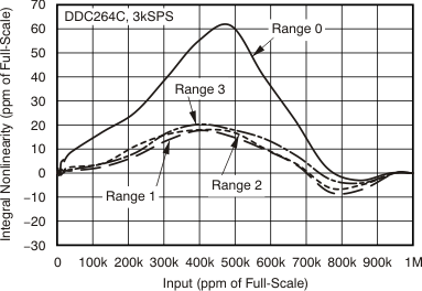
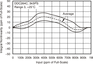
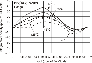
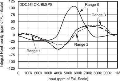
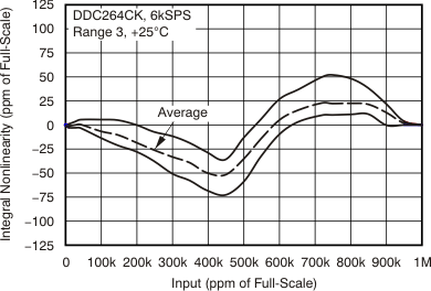
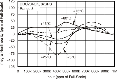
| Integral linearity error(4) | ±0.025% Reading ±1-ppm FSR | ±0.05% Reading ±1.5-ppm FSR |
|||||
| Resolution | No missing codes, format = 1 | 20 | Bits | ||||
| No missing codes, format = 0 | 16 | ||||||
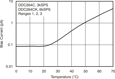
| Input bias current | TA = 25°C to 45°C | ±0.5 | ±5 | pA | |||
| Range error match(5) | 0.1% | 0.5% | FSR | ||||
| Range sensitivity to VREF | VREF = 4.096 ±0.1 V | 1:1 | |||||
| Offset error | ±500 | ±1000 | ppm of FSR | ||||
| Offset error match(5) | ±150 | ppm of FSR | |||||
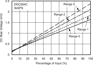
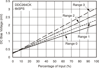
| DC bias voltage(6) | Low-level input (< 1% FSR) | ±0.1 | ±1 | mV | |||
| Power-supply rejection ratio | At DC | 100 | ±300 | ppm of FSR/V | |||
| PERFORMANCE OVER TEMPERATURE | |||||||
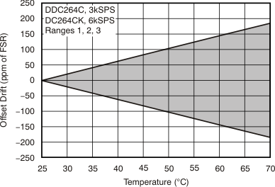
| Offset drift | ±0.5 | 5(7) | ppm of FSR/°C | ||||
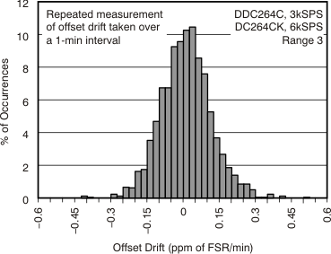
| Offset drift stability | ±0.2 | 2(7) | ppm of FSR/minute | ||||
| DC bias voltage drift(6) | ±3 | μV/°C | |||||
| Input bias current drift | TA = 25°C to 45°C | 0.01 | 1(7) | pA/°C | |||
| Range drift(8) | 25 | 50 | ppm/°C | ||||
| Range drift match(5) | ±5 | ppm/°C | |||||
| REFERENCE | |||||||
| Input current(9) | Average value with tINT = 333 µs | 825 | μA | ||||
| Average value with tINT = 166 µs (DDC264CK) | 1650 | μA | |||||
| DIGITAL INPUT AND OUTPUT | |||||||
| VIH | 0.8 × DVDD | DVDD + 0.1 | V | ||||
| VIL | –0.1 | 0.2 × DVDD | V | ||||
| VOH | IOH = –500 µA | DVDD – 0.4 | V | ||||
| VOL | IOL = 500 µA | 0.4 | V | ||||
| IIN | Input current | 0 < VIN < DVDD | ±10 | µA | |||
| Data format(10) | Straight binary | ||||||
| POWER-SUPPLY REQUIREMENTS | |||||||
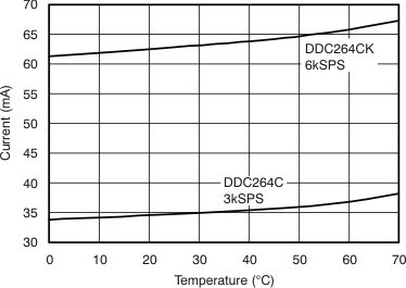
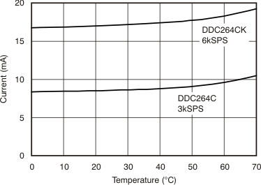
| Analog current | DDC264C | 34 | mA | ||||
| DDC264CK | 60 | ||||||
| Digital current | DDC264C | 7.5 | mA | ||||
| DDC264CK | 15 | ||||||
| Total power dissipation | DDC264C | 192 | 256 | mW | |||
| DDC264CK | 350 | ||||||
| Per channel power dissipation | DDC264C | 3 | 4 | mW/Channel | |||
| DDC264CK | 5.5 | ||||||
(1) Input is less than 1% of full-scale.
(2) CSENSOR is the capacitance seen at the DDC264 inputs from wiring, photodiode, etc.
(3) FSR is full-scale range.
(4) A best-fit line is used in measuring nonlinearity.
(5) Matching between side A and side B of the same input.
(6) Voltage produced by the DDC264 at its input that is applied to the sensor.
(7) Ensured by design; not production tested.
(8) Range drift does not include external reference drift.
(9) Input reference current decreases with increasing tINT (see Voltage Reference).
(10) Data format is straight binary with a small offset. The number of bits in the output word is controlled by the format bit.
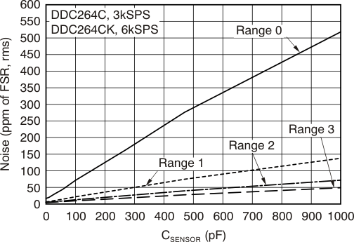
Table 1. NOISE vs CSENSOR(1)
| RANGE | CSENSOR | ||||||||
|---|---|---|---|---|---|---|---|---|---|
| 0 pF | 10 pF | 30 pF | 43 pF | 57 pF | 100 pF | 270 pF | 470 pF | 1000 pF | |
| ppm of FSR, rms | |||||||||
| Range 0: 12.5 pC | 16 | 20 | 30 | 37 | 44 | 71 | 160 | 270 | 510 |
| Range 1: 50 pC | 6.4 | 7.4 | 10 | 12 | 14 | 21 | 45 | 74 | 130 |
| Range 2: 100 pC | 5.1 | 5.5 | 7.1 | 8 | 9.1 | 12 | 25 | 39 | 71 |
| Range 3: 150 pC | 4.8 | 5 | 6 | 6.5 | 7.2 | 9.6 | 17 | 27 | 49 |
| fC, rms | |||||||||
| Range 0: 12.5 pC | 0.2 | 0.25 | 0.38 | 0.46 | 0.55 | 0.89 | 2 | 3.38 | 6.38 |
| Range 1: 50 pC | 0.32 | 0.37 | 0.53 | 0.62 | 0.73 | 1.09 | 2.29 | 3.73 | 6.88 |
| Range 2: 100 pC | 0.51 | 0.55 | 0.71 | 0.8 | 0.91 | 1.28 | 2.5 | 3.97 | 7.16 |
| Range 3: 150 pC | 0.72 | 0.75 | 0.9 | 0.98 | 1.08 | 1.45 | 2.67 | 4.14 | 7.36 |
| Electrons, rms | |||||||||
| Range 0: 12.5 pC | 1250 | 1560 | 2340 | 2890 | 3430 | 5540 | 12480 | 21070 | 39790 |
| Range 1: 50 pC | 2010 | 2310 | 3340 | 3910 | 4570 | 6800 | 14200 | 23300 | 42900 |
| Range 2: 100 pC | 3220 | 3440 | 4450 | 5000 | 5680 | 7990 | 15600 | 24800 | 44700 |
| Range 3: 150 pC | 4530 | 4730 | 5610 | 6120 | 6770 | 9050 | 16700 | 25800 | 45900 |
(1) Noise in Table 1 is expressed in three different units for reader convenience. The first section lists noise in units of parts per million of full-scale range; the second section shows noise as an equivalent input charge (in fC); and the third section converts noise to electrons.
7.6 Typical Characteristics
at TA = 25°C (unless otherwise noted)