SBAS368D May 2006 – December 2016 DDC264
PRODUCTION DATA.
- 1 Features
- 2 Applications
- 3 Description
- 4 Revision History
- 5 Device Comparison Table
- 6 Pin Configuration and Functions
- 7 Specifications
-
8 Detailed Description
- 8.1 Overview
- 8.2 Functional Block Diagram
- 8.3
Feature Description
- 8.3.1 Dual Switched Integrator: Basic Integration Cycle
- 8.3.2 Integration Capacitors
- 8.3.3 Voltage Reference
- 8.3.4 Serial Data Output and Control Interface
- 8.4 Device Functional Modes
- 8.5 Programming
- 8.6 Register Maps
- 9 Application and Implementation
- 10Power Supply Recommendations
- 11Layout
- 12Device and Documentation Support
- 13Mechanical, Packaging, and Orderable Information
9 Application and Implementation
NOTE
Information in the following applications sections is not part of the TI component specification, and TI does not warrant its accuracy or completeness. TI’s customers are responsible for determining suitability of components for their purposes. Customers should validate and test their design implementation to confirm system functionality.
9.1 Application Information
A typical application case of the DDC family of products, including the DDC264, is the measurement of currents produced by photodiodes when excited by light, or the equivalent charge over a period of time (see Equation 5). The DDC264 can measure 64 channels simultaneously. As explained in Functional Block Diagram, the measurement is done by integrating the currents during a given time, set by the two consecutive edges of the CONV signal, provided by the system, see Figure 19. The result of the integration is shown in Equation 5.

where
- ti and tf represent the instant where the integration starts and finishes, respectively
- i(t) the input current (which is a function of time)
- Q the reported result by the DDC
All temporal information of i in that interval is lost and only an equivalent average i can be obtained.
The user must also provide a CLK signal used to run all the internal circuits, including the ADCs, which converts the result of the integration and generate a DVALID pulse to indicate that the conversion is done. The controller, then, can read that data, before it gets erased by the next conversion. The following sections explain the necessary control signals to operate the device, and the choices that the circuit designer can make.
9.2 Typical Application
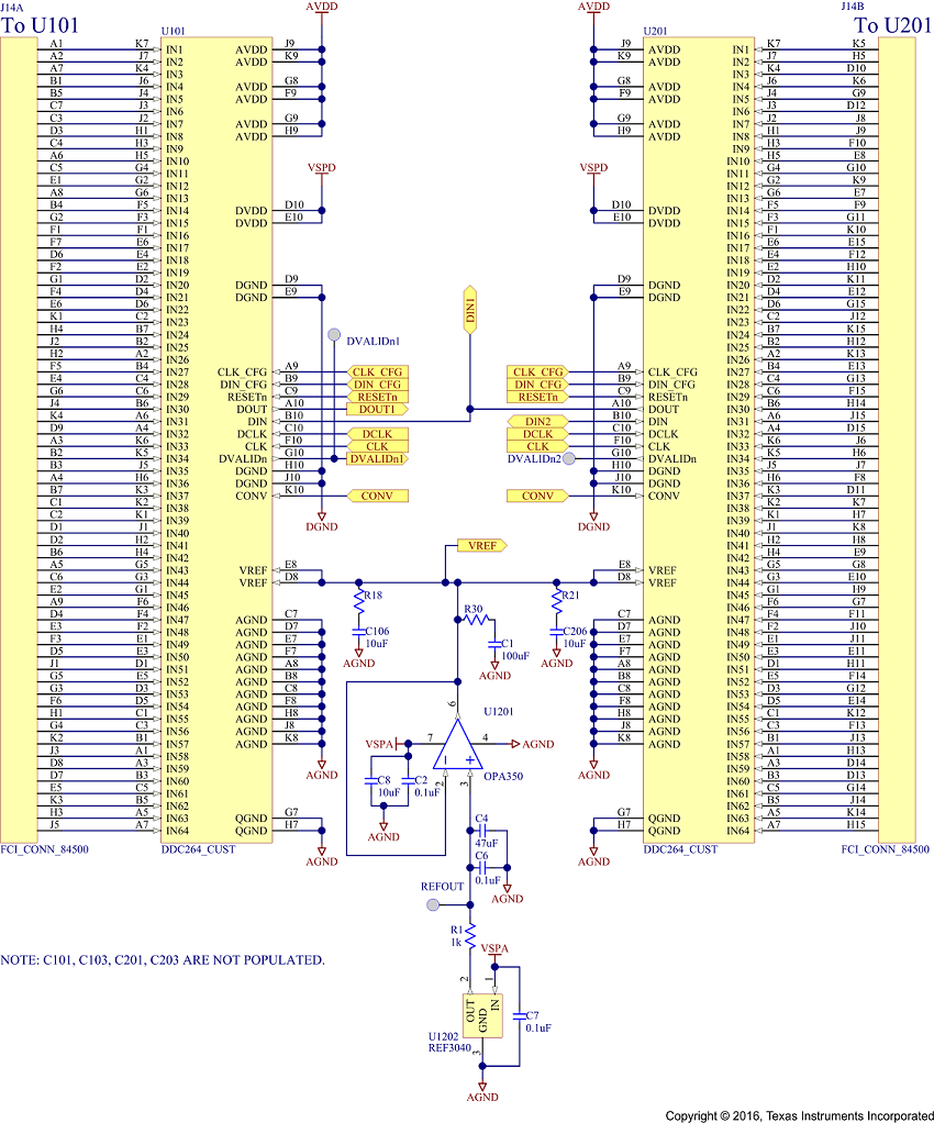
 Figure 31. Typical Application Circuit
9.2.1 Design Requirements
For the following example, assume the user wants to measure the current coming from 128 photodiodes every 500 µs, and the maximum current per photodiode is 250 nA.
9.2.2 Detailed Design Procedure
9.2.2.1 Input Connection
Figure 31 represents a top level schematic of a solution for this case. 2 DDC264 are used. Inputs are represented on the top schematic by the two connectors on the left and right sides.
The photodiodes must be connected to the inputs in such a way that the current flows into the device. To achieve that, usually the anode of the photodiode is connected to the input of the device (see Figure 20) and the cathode to a node with the same or higher voltage, in such a way that the photodiode is reverse biased or not biased at all. The application usually determines the choice. No bias minimizes dark current in the photodiode; therefore, minimizing errors during the integration or measurement of small signal currents. Nevertheless, the parasitic junction capacitance of the photodiode decreases with the reverse bias voltage. The lower the input capacitance, the lower the input noise (see Table 1). As such, applying a reverse bias reduces the noise of the measurement while increasing the dark current. The user must choose depending on their application. In applications with small signal currents, usually no bias is applied. In that case, the cathodes can be connected to AGND.
Notice that although only positive currents (in the direction towards the inside of the device) can be measured, the device has around 0.4% margin towards the negative excursion. In this way, small offsets and negative currents do not saturate the device in the bottom rail and can be detected and measured.
9.2.2.2 Selecting Integration Time, Device Clock, and Range
The second step is to select the right integration time. There may be system level constraints that set this. For instance, to get at least a given number of readings per second. Going faster than that may not be helpful, degrade performance and increase power unnecessarily. In this case, the user wants to, at least, get 2 KSPS (integration time = 500 µs). With 500 µs, the maximum integrated charge would be 250 nA × 500 µs = 125 pC. This is too much for Range 2 (100 pC full scale) but falls comfortably in Range 3 (150 pC). As such, the likely preferred option is to use Range 3 by setting bits 9 and 10 to one. Another potential option is to run the device slightly faster such that Range 2 can be used. In this case, 100 pC/250 nA = 400 µs, or 2.5 KSPS. Notice that this frequency (the frequency at which input currents are sampled) is actually 2× the frequency of the CONV signal. That is, 400 µs is half the period of the CONV signal, i.e. the time between two consecutive edges of the CONV signal.
The user must check the specification and performance curves to see the differences between both ranges for the specific conditions. Normally, performance may be close in both cases and operating the device slower may give some extra advantage on power and help relax practical system constraints.
For this particular case, both choices can be supported with the lower speed version device (DDC264C version), which supports up to 3 KSPS. As such, to benefit from this, the user must set bit 7 to zero. In this mode, the maximum internal clock is 5 MHz, so the user can choose to drive the CLK pin of the device with a 5-MHz clock maximum or with a 20-MHz clock maximum and the internal divide by 4 (setting register bit 13 to one).
Notice that using a slower external clock is also possible, but the ADC conversion lasts longer (see tDR in Table 2). This affects the time left to capture data after DVALID and before CONV edge (see Reading the Measurement)
9.2.2.3 Voltage Reference
It is critical that VREF be stable during the different modes of operation (see Figure 22). The A/D converter measures the voltage on the integrator with respect to VREF. Because the integrator capacitors are initially reset to VREF, any drop in VREF from the time the capacitors are reset to the time when the converter measures the integrator output introduces an offset. It is also important that VREF be stable over longer periods of time because changes in VREF correspond directly to changes in the full-scale range. Finally, VREF must introduce as little additional noise as possible.
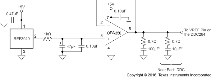
For these reasons, it is strongly recommended that the external reference source be buffered with an operational amplifier, as shown in Figure 32. In this circuit, the voltage reference is generated by a +4.096 V reference. A low-pass filter to reduce noise connects the reference to an operational amplifier configured as a buffer. This amplifier must have low noise and input/output common-mode ranges that support VREF. Even though the circuit in Figure 32 might appear to be unstable because of the large output capacitors, it works well for the OPA350. TI does not recommend a series resistor be placed at its output to improve stability, because this can cause a drop in VREF which produces large offsets. 10 µF and 0.7 Ω are good initial values for the decoupling network close to the DDC264, but may have to be optimized depending on its placement and board layout.

Figure 31 shows a portion of the driving circuit on the top part, driving one of the DDC264. This assumes that the output of the reference IC is routed from somewhere else, due, for instance, to space limitations on the board. Being the reference noise critical for the final performance of the system, TI recommends shielding and passing the filter the signal low. The bottom of Figure 31 shows the second DDC264 where the reference is driven by the same buffer as the first DDC and only a decoupling network is added close to the device. This is again assuming space and cost limitations. Ideally the use of two different buffers, one close to each reference, isolates interactions between both devices from being coupled through the reference line.
9.2.2.4 Reading the Measurement
As explained in Data Retrieval, the data can be read as soon as DVALID goes low. The user can choose to monitor this signal or simply wait a period of time predicted by tDR in Table 2. For this example, assuming that a CLK frequency of 5 MHz was selected, the data would be ready after approximately 276 µs. Staying with Range 3, the integration time is 500 µs and as such, after detecting DVALID, there is approximately 500 µs – 276 µs to read the data. We assume 220 µs to avoid getting too close to the CONV edge. In 20 bit mode, reading two DDC264, with daisy chain between DOUT and DIN, see Figure 31, would take 128 × 20 × (1/32 MHz) = 80 µs, which fits in the interval between DVALID and next CONV edge. This minimizes noise due to the DCLK and DOUT switching during the conversion of the ADC (which happens from CONV edge to /DVALID) and can help improve the performance. In Figure 31, both converters are connected in daisy chain, which minimizes the number of traces being routed back to the controller. One small drawback of this approach versus shifting the data of both DDC264 in parallel (without the daisy chain) is that the outputs switch for longer time (2×), increasing the total power by a small fraction (as the output switching power is only a small portion of the total power consumption). Another solution is to transfer part or all the data during the ADC conversion (see Retrieval Before and After CONV Toggles and Retrieval After CONV Toggles). A potential way to minimize this noise, specially if the DOUT traces are long is to buffer them on board, close to the device.
9.2.3 Application Curve
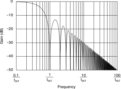
The frequency response of the DDC264 is set by the front-end integrators and is that of a traditional continuous time integrator, as shown in Figure 33. By adjusting the integration time, tINT, the user can change the 3-dB bandwidth and the location of the notches in the response. The frequency response of the A/D converter that follows the front-end integrator is of no consequence because the converter samples a held signal from the integrators. That is, the input to the A/D converter is always a DC signal. The output of the front-end integrators are sampled; therefore, aliasing can occur. Whenever the frequency of the input signal exceeds one-half of the sampling rate the signal folds back down to lower frequencies.
 Figure 33. Frequency Response