ZHCSKH5C May   2008  – November 2019 DAC9881

PRODUCTION DATA.  

  1. 特性
  2. 应用
  3. 说明
    1.     Device Images
      1.      方框图
  4. 修订历史记录
  5. Pin Configuration and Functions
    1.     Pin Functions
  6. Specifications
    1. 6.1  Absolute Maximum Ratings
    2. 6.2  ESD Ratings
    3. 6.3  Recommended Operating Conditions
    4. 6.4  Thermal Information
    5. 6.5  Electrical Characteristics: AVDD = 5 V
    6. 6.6  Electrical Characteristics: AVDD = 2.7 V
    7. 6.7  Timing Requirements—Standalone Operation Without SDO
    8. 6.8  Timing Requirements—Standalone Operation With SDO and Daisy-Chain Mode
    9. 6.9  Typical Characteristics: AVDD = 5 V
    10. 6.10 Typical Characteristics: AVDD = 2.7 V
  7. Detailed Description
    1. 7.1 Overview
    2. 7.2 Functional Block Diagram
    3. 7.3 Feature Description
      1. 7.3.1  Analog Output
      2. 7.3.2  Reference Inputs
      3. 7.3.3  Output Range
      4. 7.3.4  Input Data Format
      5. 7.3.5  Hardware Reset
      6. 7.3.6  Power-On Reset
        1. 7.3.6.1 Program Reset Value
      7. 7.3.7  Power Down
      8. 7.3.8  Double-Buffered Interface
        1. 7.3.8.1 Load DAC Pin (LDAC)
          1. 7.3.8.1.1 Synchronous Mode
          2. 7.3.8.1.2 Asynchronous Mode
      9. 7.3.9  1.8-V to 5-V Logic Interface
      10. 7.3.10 Power-Supply Sequence
    4. 7.4 Device Functional Modes
      1. 7.4.1 Serial Interface
        1. 7.4.1.1 Input Shift Register
          1. 7.4.1.1.1 Stand-Alone Mode
          2. 7.4.1.1.2 Daisy-Chain Mode
  8. Application and Implementation
    1. 8.1 Application Information
      1. 8.1.1 Bipolar Operation Using the DAC9881
    2. 8.2 Typical Application
      1. 8.2.1 DAC9881 Sample-and-Hold Circuit
        1. 8.2.1.1 Design Requirements
        2. 8.2.1.2 Detailed Design Procedure
        3. 8.2.1.3 Application Curves
    3. 8.3 System Example
  9. Power Supply Recommendations
  10. 10Layout
    1. 10.1 Layout Guidelines
    2. 10.2 Layout Example
  11. 11器件和文档支持
    1. 11.1 文档支持
      1. 11.1.1 相关文档
    2. 11.2 接收文档更新通知
    3. 11.3 支持资源
    4. 11.4 商标
    5. 11.5 静电放电警告
    6. 11.6 Glossary
  12. 12机械、封装和可订购信息

封装选项

机械数据 (封装 | 引脚)
散热焊盘机械数据 (封装 | 引脚)
订购信息

Application Curves

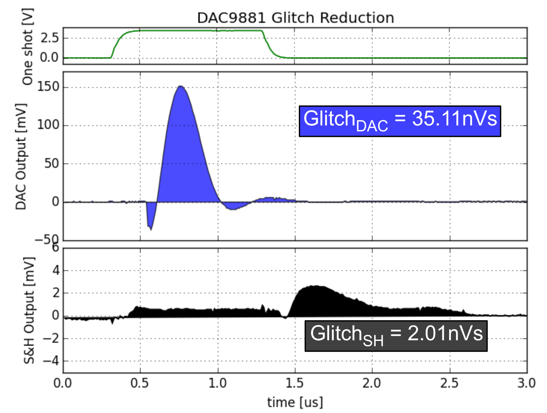
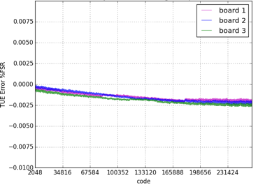
Glitch reduction and total unadjusted error (TUE) plots of the solution presented in Sample and Hold Glitch Reduction for Precision Outputs Design Guide (TIDU022) is shown in the following plots. The glitch area is reduced from 35.11 nVs to 2.01 nVs.
DAC9881 fig_24_sbas337.png
Figure 73. DAC9881 Sample-and-Hold TUE Error %FSR
DAC9881 fig_33_sbas337.png
CH = 8.2 nF RS = 14.7 Ω
Figure 74. Measured Glitch Area (20000h-1FFFFh)
(Top) Digital Signal One-Shot Pulse; (Middle) DAC Output Glitch; (Bottom) S-H Output Glitch