ZHCSHP3 February 2018 DAC8771
PRODUCTION DATA.
- 1 特性
- 2 应用
- 3 说明
- 4 修订历史记录
- 5 Device Comparison Table
- 6 Pin Configuration and Functions
- 7 Specifications
-
8 Detailed Description
- 8.1 Overview
- 8.2 Functional Block Diagram
- 8.3
Feature Description
- 8.3.1 Current Output Stage
- 8.3.2 Voltage Output Stage
- 8.3.3 Buck-Boost Converter
- 8.3.4 Analog Power Supply
- 8.3.5 Digital Power Supply
- 8.3.6 Internal Reference
- 8.3.7 Power-On-Reset
- 8.3.8 ALARM Pin
- 8.3.9 Power GOOD bit
- 8.3.10 Status Register
- 8.3.11 Status Mask
- 8.3.12 Alarm Action
- 8.3.13 Watchdog Timer
- 8.3.14 Programmable Slew Rate
- 8.3.15 HART Interface
- 8.4 Device Functional Modes
- 8.5
Register Maps
- 8.5.1
Register Maps
- 8.5.1.1 DAC8771 Commands
- 8.5.1.2
Register Maps and Bit Functions
- 8.5.1.2.1 No Operation Register (address = 0x00) [reset = 0x0000]
- 8.5.1.2.2 Reset Register (address = 0x01) [reset = 0x0000]
- 8.5.1.2.3 Reset Config Register (address = 0x02) [reset = 0x0000]
- 8.5.1.2.4 Select DAC Register (address = 0x03) [reset = 0x0000]
- 8.5.1.2.5 Configuration DAC Register (address = 0x04) [reset = 0x0000]
- 8.5.1.2.6 DAC Data Register (address = 0x05) [reset = 0x0000]
- 8.5.1.2.7 Select Buck-Boost Converter Register (address = 0x06) [reset = 0x0000]
- 8.5.1.2.8 Configuration Buck-Boost Register (address = 0x07) [reset = 0x0000]
- 8.5.1.2.9 DAC Channel Calibration Enable Register (address = 0x08) [reset = 0x0000]
- 8.5.1.2.10 DAC Channel Gain Calibration Register (address = 0x09) [reset = 0x0000]
- 8.5.1.2.11 DAC Channel Offset Calibration Register (address = 0x0A) [reset = 0x0000]
- 8.5.1.2.12 Status Register (address = 0x0B) [reset = 0x1000]
- 8.5.1.2.13 Status Mask Register (address = 0x0C) [reset = 0x0000]
- 8.5.1.2.14 Alarm Action Register (address = 0x0D) [reset = 0x0000]
- 8.5.1.2.15 User Alarm Code Register (address = 0x0E) [reset = 0x0000]
- 8.5.1.2.16 Reserved Register (address = 0x0F) [reset = N/A]
- 8.5.1.2.17 Write Watchdog Timer Register (address = 0x10) [reset = 0x0000]
- 8.5.1.2.18 Reserved Register (address 0x12 - 0xFF) [reset = N/A]
- 8.5.1
Register Maps
- 9 Application and Implementation
- 10Power Supply Recommendations
- 11Layout
- 12器件和文档支持
- 13机械、封装和可订购信息
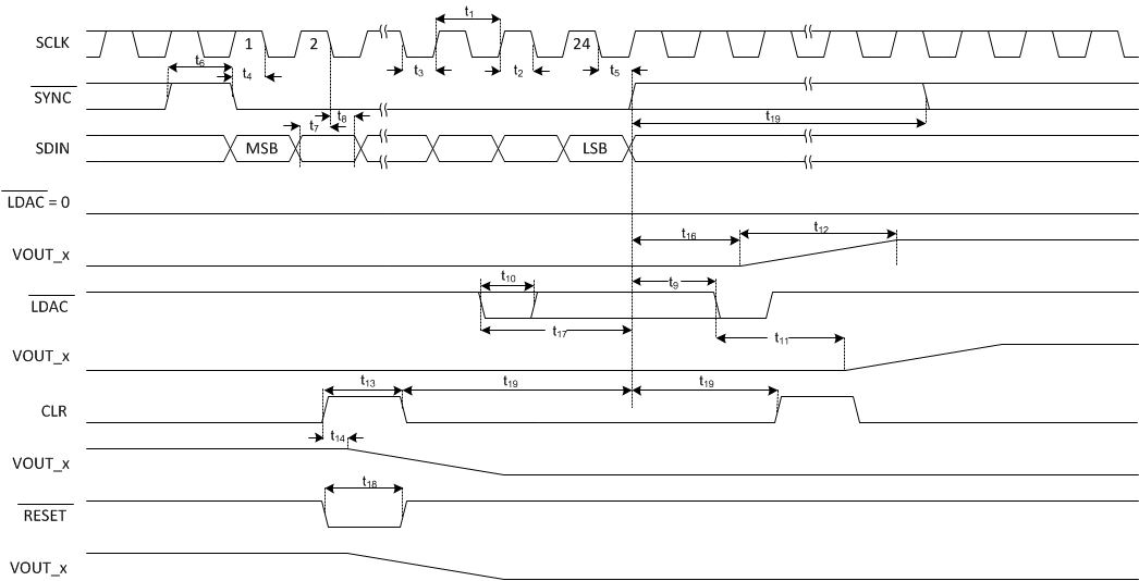
7.6 Timing Requirements: Write and Readback Mode
At TA = –40°C to +125°C and DVDD = +2.7 V to +5.5 V, unless otherwise noted.| PARAMETER | TEST CONDITIONS | MIN | MAX | UNIT | |
|---|---|---|---|---|---|
| fSCLK | Max clock frequency | 25 | MHz | ||
| t1 | SCLK cycle time | 40 | ns | ||
| t2 | SCLK high time | 18 | ns | ||
| t3 | SCLK low time | 18 | ns | ||
| t4 | SYNC falling edge to SCLK falling edge setup time | 15 | ns | ||
| t5 | 24th/32nd SCLK falling edge to SYNC rising edge | 13 | ns | ||
| t6 | SYNC high time | Digital slew rate control disabled | 40 | ns | |
| t7 | Data setup time | 8 | ns | ||
| t8 | Data hold time | 5 | ns | ||
| t9 | SYNC rising edge to LDAC falling edge | 33 | ns | ||
| t10 | LDAC pulse width low | 10 | ns | ||
| t11 | LDAC falling edge to DAC output response time | 50 | ns | ||
| t12 | DAC output settling time | See section 5.3 | µs | ||
| t13 | CLR high time | 10 | ns | ||
| t14 | CLR activation time | 50 | ns | ||
| t15 | SCLK rising edge to SDO valid | 14 | ns | ||
| t16 | SYNC rising edge to DAC output response time | 50 | ns | ||
| t17 | LDAC falling edge to SYNC rising edge | 100 | ns | ||
| t18 | RESET pulse width | 10 | ns | ||
| t19 | SYNC rising edge to CLR falling/rising edge | 60 | ns | ||
 Figure 1. Write Mode Timing
 Figure 2. Readback Mode Timing