ZHCSB25B April 2013 – January 2017 DAC3174
PRODUCTION DATA.
- 1 特性
- 2 应用
- 3 说明
- 4 修订历史记录
- 5 Pin Configuration and Functions
-
6 Specifications
- 6.1 Absolute Maximum Ratings
- 6.2 ESD Ratings
- 6.3 Recommended Operating Conditions
- 6.4 Thermal Information
- 6.5 Electrical Characteristics: DC Specifications
- 6.6 Electrical Characteristics: AC Specifications
- 6.7 Electrical Characteristics: Digital Specifications
- 6.8 Timing Requirements
- 6.9 Typical Characteristics
-
7 Detailed Description
- 7.1 Overview
- 7.2 Functional Block Diagrams
- 7.3 Feature Description
- 7.4 Device Functional Modes
- 7.5 Programming
- 7.6
Register Maps
- 7.6.1 config0 Register (address = 0x00) [reset = 0x44FC]
- 7.6.2 config 1 Register (address = 0x01) [reset = 0x600E]
- 7.6.3 config2 Register (address = 0x02) [reset = 0x3FFF]
- 7.6.4 config3 Register (address = 0x03) [reset = 0x0000]
- 7.6.5 config4 Register (address = 0x04) [reset = 0x0000]
- 7.6.6 config5 Register (address = 0x05) [reset = 0x0000]
- 7.6.7 config6 Register (address = 0x06) [reset = 0x0000]
- 7.6.8 config7 Register (address = 0x07) [reset = 0xFFFF]
- 7.6.9 config8 Register (address = 0x08) [reset = 0x4000]
- 7.6.10 config9 Register (address = 0x09) [reset = 0x8000]
- 7.6.11 config10 Register (address = 0x0A) [reset = 0xF080]
- 7.6.12 config11 Register (address = 0x0B) [reset = 0x1111]
- 7.6.13 config12 Register (address = 0x0C) [reset = 0x3A7A]
- 7.6.14 config13 Register (address = 0x0D) [reset = 0x36B6]
- 7.6.15 config14 Register (address = 0x0E) [reset = 0x2AEA]
- 7.6.16 config15 Register (address = 0x0F) [reset = 0x0545]
- 7.6.17 config16 Register (address = 0x10) [reset = 0x0585]
- 7.6.18 config17 Register (address = 0x11) [reset = 0x0949]
- 7.6.19 config18 Register (address = 0x12) [reset = 0x1515]
- 7.6.20 config19 Register (address = 0x13) [reset = 0x3ABA]
- 7.6.21 config20 Register (address = 0x14) [reset = 0x0000]
- 7.6.22 config21 Register (address = 0x15) [reset = 0xFFFF]
- 7.6.23 config22 Register (address = 0x16) [reset = N/A]
- 7.6.24 config23 Register (address = 0x17) [reset = N/A]
- 7.6.25 config24 Register (address = 0x18) [reset = N/A]
- 7.6.26 config25 Register (address = 0x19) [reset = N/A]
- 7.6.27 config127 Register (address = 0x7F) [reset = 0x0045]
- 8 Application and Implementation
- 9 Power Supply Recommendations
- 10Layout
- 11器件和文档支持
- 12机械、封装和可订购信息
10 Layout
10.1 Layout Guidelines
- DAC output termination resistors must be placed as close to the output pins as possible to provide a dc path to ground and set the source impedance.
- Route the LVDS data signals as impedance-controlled, tightly-coupled, matched-length differential traces.
- Maintain a solid ground plane under the LVDS signals without any ground plane splits.
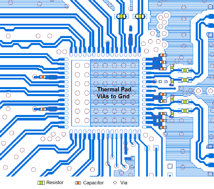
- Place a thermal ground pad under the device with an adequate number of vias to the ground planes of the board.
10.2 Layout Example
 Figure 59. DAC3174 Layout Example