ZHCSDM6A JUNE   2013  – December 2014 DAC161S997

PRODUCTION DATA.  

  1. 特性
  2. 应用
  3. 说明
  4. 简化电路原理图
  5. 修订历史记录
  6. Pin Configuration and Functions
  7. Specifications
    1. 7.1 Absolute Maximum Ratings
    2. 7.2 ESD Ratings
    3. 7.3 Recommended Operating Conditions
    4. 7.4 Thermal Information
    5. 7.5 Electrical Characteristics
    6. 7.6 Timing Requirements
    7. 7.7 Typical Characteristics
  8. Detailed Description
    1. 8.1 Overview
    2. 8.2 Functional Block Diagram
    3. 8.3 Feature Description
      1. 8.3.1 Error Detection And Reporting
        1. 8.3.1.1 Loop Error
        2. 8.3.1.2 SPI Timeout Error (Channel Error)
        3. 8.3.1.3 Frame Error
        4. 8.3.1.4 Alarm Current
    4. 8.4 Device Functional Modes
    5. 8.5 Programming
      1. 8.5.1 Serial Interface
        1. 8.5.1.1 SPI Write
        2. 8.5.1.2 SPI Read
        3. 8.5.1.3 Optional Protected SPI Writes
          1. 8.5.1.3.1 SPI Write Error Correction
    6. 8.6 Register Maps
  9. Application and Implementation
    1. 9.1 Application Information
      1. 9.1.1 16-bit Dac And Loop Drive
        1. 9.1.1.1 DC Characteristics
        2. 9.1.1.2 DC Input-Output Transfer Function
        3. 9.1.1.3 Loop Interface
        4. 9.1.1.4 Loop Compliance
        5. 9.1.1.5 AC Characteristics
          1. 9.1.1.5.1 Step Response
          2. 9.1.1.5.2 Output Impedance
          3. 9.1.1.5.3 PSRR
          4. 9.1.1.5.4 Stability
          5. 9.1.1.5.5 Noise and Ripple
          6. 9.1.1.5.6 Digital Feedthrough
          7. 9.1.1.5.7 HART Signal Injection
          8. 9.1.1.5.8 RC Filter Limitation
    2. 9.2 Typical Application
      1. 9.2.1 Design Requirements
      2. 9.2.2 Detailed Design Procedure
        1. 9.2.2.1 Reasons for Choosing a 3.9-V Zener Diode
        2. 9.2.2.2 Loop Compliance Voltage
        3. 9.2.2.3 Selection of External BJT
      3. 9.2.3 Application Curve
  10. 10Power Supply Recommendations
  11. 11Layout
    1. 11.1 Layout Guidelines
    2. 11.2 Layout Example
  12. 12器件和文档支持
    1. 12.1 商标
    2. 12.2 静电放电警告
    3. 12.3 术语表
  13. 13机械、封装和可订购信息

封装选项

机械数据 (封装 | 引脚)
散热焊盘机械数据 (封装 | 引脚)
订购信息

11 Layout

11.1 Layout Guidelines

To maximize the performance of the DAC161S997 in any application, good layout practices and proper circuit design must be followed. A few recommendations specific to the DAC161S997 are:

  • Make sure that VD and VA have decoupling capacitors local to the respective terminals.
  • Minimize trace length between the C1, C2, and C3 capacitors and the DAC161S997 pins.
11.2 Layout Example

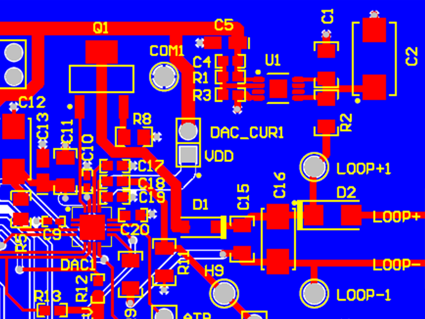
Figure 30 to Figure 32 show the DAC161S997 evaluation module (EVM) layout

DAC161S997 lay01_top_assembly_snas621.pngFigure 30. Example PCB layout: Top Assembly Layer
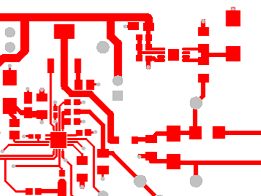
DAC161S997 lay02_top_routing_snas621.pngFigure 31. Example PCB layout: Top Layer
DAC161S997 lay03_bot_routing_snas621.pngFigure 32. Example PCB layout: Bottom Layer