SNAS410F May 2008 – July 2016 DAC121S101QML-SP
PRODUCTION DATA.
- 1 Features
- 2 Applications
- 3 Description
- 4 Revision History
- 5 Pin Configuration and Functions
-
6 Specifications
- 6.1 Absolute Maximum Ratings
- 6.2 ESD Ratings
- 6.3 Recommended Operating Conditions
- 6.4 Thermal Information
- 6.5 DAC121S101QML-SP Electrical Characteristics DC Parameters
- 6.6 DAC121S101QML-SP Electrical Characteristics AC and Timing Characteristics
- 6.7 DAC121S101QML Electrical Characteristics Radiation Electrical Characteristics
- 6.8 DAC121S101QML-SP Electrical Characteristics Operating Life Test Delta Parameters TA at 25°C
- 6.9 Typical Characteristics
- 7 Detailed Description
- 8 Application and Implementation
- 9 Power Supply Recommendations
- 10Layout
- 11Device and Documentation Support
- 12Mechanical, Packaging, and Orderable Information
8 Application and Implementation
NOTE
Information in the following applications sections is not part of the TI component specification, and TI does not warrant its accuracy or completeness. TI’s customers are responsible for determining suitability of components for their purposes. Customers should validate and test their design implementation to confirm system functionality.
8.1 Application Information
The simplicity of the DAC121S101QML-SP implies ease of use. However, it is important to recognize that any data converter that uses its supply voltage as its reference voltage will have essentially zero PSRR (Power Supply Rejection Ratio). Therefore, it is necessary to provide a noise-free supply voltage to the device.
8.1.1 Bipolar Operation
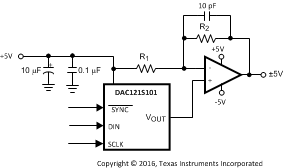
The DAC121S101QML-SP is designed for single-supply operation and thus has a unipolar output. However, a bipolar output may be obtained with the circuit in Figure 33. This circuit will provide an output voltage range of
±5 V. A rail-to-rail amplifier must be used if the amplifier supplies are limited to ±5 V.
 Figure 33. Bipolar Operation
The output voltage of this circuit for any code is found to be:
where
- D is the input code in decimal form
With VA = 5 V and R1 = R2,
8.1.2 DSP and Microprocessor Interfacing
Interfacing the DAC121S101QML-SP to microprocessors and DSPs is quite simple. The following guidelines are offered to hasten the design process.
8.1.2.1 ADSP-2101/ADSP2103 Interfacing
Figure 34 shows a serial interface between the DAC121S101QML-SP and the ADSP-2101/ADSP2103. The DSP must be set to operate in the SPORT Transmit Alternate Framing Mode. It is programmed through the SPORT control register and should be configured for Internal Clock Operation, Active Low Framing and 16-bit Word Length. Transmission is started by writing a word to the Tx register after the SPORT mode has been enabled.
 Figure 34. ADSP-2101/2103 Interface
8.1.2.2 80C51/80L51 Interface
Figure 35 shows a serial interface between the DAC121S101QML-SP and the 80C51/80L51 microcontroller. The SYNC signal comes from a bit-programmable pin on the microcontroller. The example shown here uses port line P3.3. This line is taken low when data is to transmitted to the DAC121S101QML-SP. Because the 80C51/80L51 transmits 8-bit bytes, only eight falling clock edges occur in the transmit cycle. To load data into the DAC, the P3.3 line must be left low after the first eight bits are transmitted. A second write cycle is initiated to transmit the second byte of data, after which port line P3.3 is brought high. The 80C51/80L51 transmit routine must recognize that the 80C51/80L51 transmits data with the LSB first while the DAC121S101QML-SP requires data with the MSB first.
 Figure 35. 80C51/80L51 Interface
8.1.2.3 68HC11 Interface
Figure 36 shows a serial interface between the DAC121S101QML-SP and the 68HC11 microcontroller. The SYNC line of the DAC121S101QML-SP is driven from a port line (PC7 in the figure), similar to the 80C51/80L51.
The 68HC11 must be configured with its CPOL bit as a zero and its CPHA bit as a one. This configuration causes data on the MOSI output to be valid on the falling edge of SCLK. PC7 is taken low to transmit data to the DAC. The 68HC11 transmits data in 8-bit bytes with eight falling clock edges. Data is transmitted with the MSB first. PC7 must remain low after the first eight bits are transferred. A second write cycle is initiated to transmit the second byte of data to the DAC, after which PC7 must be raised to end the write sequence.
 Figure 36. 68HC11 Interface
8.1.2.4 Microwire Interface
Figure 37 shows an interface between a Microwire-compatible device and the DAC121S101QML-SP. Data is clocked out on the rising edges of the SCLK signal.
 Figure 37. Microwire Interface
8.1.3 Radiation Environments
Carefully consider the environmental conditions when using a product in a radiation environment. Radiation on test reports are available on TI.com/radiation.
8.1.3.1 Total Ionizing Dose
The products with the radiation hardness assurance (RHA) levels listed in the are qualified for low dose rate environments only.
8.1.3.1.1 DAC121S101WGRQV 5962R0722601VZA
This product is tested and qualified per MIL-STD-883 Test Method 1019, Condition A and the extended room temperature anneal test where a high-dose irradiation followed by a room temperature anneal is used to simulate a dose rate of 0.027 rad(Si)/s and is qualified for environments with radiation levels of 0.027 rad(Si)/s or lower.
8.1.3.1.2 DAC121S101WGRLV 5962R0722602VZA
This product is tested and qualified per MIL-STD-883 Test Method 1019, Condition D at a dose rate of 0.01 rad(Si)/s and are qualified for environments with radiation levels of 0.01 rad(Si)/s or lower.
8.1.3.2 Single Event Latch-Up and Functional Interrupt
One-time single event latch-up (SEL) and single event functional interrupt (SEFI) testing was preformed according to EIA/JEDEC Standard, EIA/JEDEC57. The linear energy transfer threshold (LETth) shown in Features is the maximum LET tested. A test report is available upon request.
8.1.3.3 Single Event Upset
A report on single event upset (SEU) is available at TI.com/radiation.
8.2 Typical Application
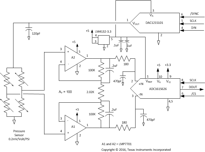
 Figure 38. Pressure Sensor Gain Adjust
8.2.1 Design Requirements
The DAC121S101QML-SP is a positive supply-only data acquisition system capable of digitizing a pressure sensor output. In addition to digitizing the pressure sensor output, the system designer can use the DAC121S101 to correct for gain errors in the pressure sensor output by adjusting the bias voltage to the bridge pressure sensor.
8.2.2 Detailed Design Procedure
As shown in Equation 4, the output of the pressure sensor is relative to the imbalance of the resistive bridge times the output of the DAC121S101, thus providing the desired gain correction.
Likewise for the ADC161S626, Equation 5 shows that the ADC output is function of the Pressure Sensor Output times relative to the ratio of the ADC input divided by the DAC121S101 output voltage.
8.2.3 Application Curve
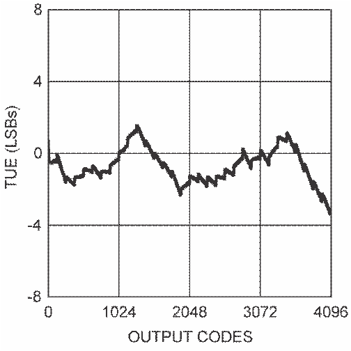
 Figure 39. Total Unadjusted Error vs Output Code