ZHCSDF5A
December 2014 – May 2024
CSD85301Q2
PRODUCTION DATA
1
1
特性
2
应用
3
说明
4
Specifications
4.1
Electrical Characteristics
4.2
Thermal Information
4.3
Typical MOSFET Characteristics
5
Device and Documentation Support
5.1
接收文档更新通知
5.2
支持资源
5.3
Trademarks
5.4
静电放电警告
5.5
术语表
6
Revision History
7
Mechanical, Packaging, and Orderable Information
7.1
Package Dimensions
7.2
PCB Land Pattern
7.3
Recommended Stencil Opening
7.4
Q2 Tape and Reel Information
封装选项
机械数据 (封装 | 引脚)
DLV|6
散热焊盘机械数据 (封装 | 引脚)
订购信息
zhcsdf5a_oa
zhcsdf5a_pm
4.3
Typical MOSFET Characteristics
(T
A
= 25°C unless otherwise stated)
Figure 4-1
Transient Thermal Impedance
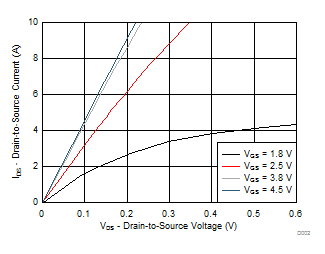
Figure 4-2
Saturation Characteristics
I
D
= 5A
V
DS
= 10V
Figure 4-4
Gate Charge
I
D
= 5A
Figure 4-6
Threshold Voltage vs Temperature
I
D
= 5A
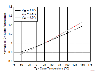
Figure 4-8
Normalized On-State Resistance vs Temperature
Single Pulse, Max R
θJA
= 185°C/W
Figure 4-10
Maximum Safe Operating Area
Figure 4-12
Maximum Drain Current vs Temperature
V
DS
= 5V
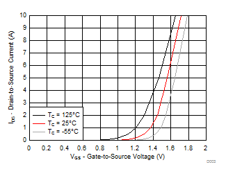
Figure 4-3
Transfer Characteristics
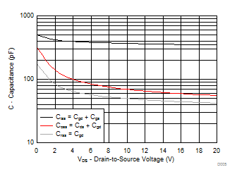
Figure 4-5
Capacitance
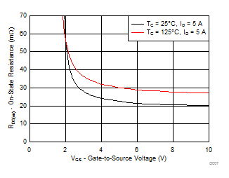
Figure 4-7
On-State Resistance vs Gate-to-Source Voltage
Figure 4-9
Typical Diode Forward Voltage
Figure 4-11
Single Pulse Unclamped Inductive Switching