ZHCSCG4 May 2014 CSD19534Q5A
PRODUCTION DATA.
5 Specifications
5.1 Electrical Characteristics
(TA = 25°C unless otherwise stated)| PARAMETER | TEST CONDITIONS | MIN | TYP | MAX | UNIT | ||
|---|---|---|---|---|---|---|---|
| STATIC CHARACTERISTICS | |||||||
| BVDSS | Drain-to-Source Voltage | VGS = 0 V, ID = 250 μA | 100 | V | |||
| IDSS | Drain-to-Source Leakage Current | VGS = 0 V, VDS = 80 V | 1 | μA | |||
| IGSS | Gate-to-Source Leakage Current | VDS = 0 V, VGS = 20 V | 100 | nA | |||
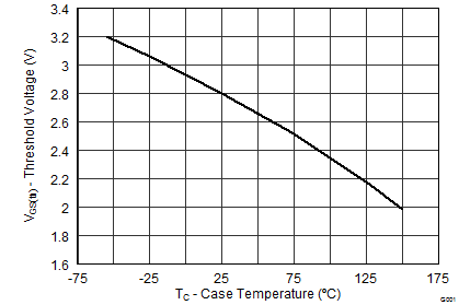
| VGS(th) | Gate-to-Source Threshold Voltage | VDS = VGS, ID = 250 μA | 2.4 | 2.8 | 3.4 | V | |
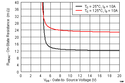
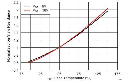
| RDS(on) | Drain-to-Source On Resistance | VGS = 6 V, ID = 10 A | 14.1 | 17.6 | mΩ | ||
| VGS = 10 V, ID = 10 A | 12.6 | 15.1 | mΩ | ||||
| gfs | Transconductance | VDS = 10 V, ID = 10 A | 47 | S | |||
| DYNAMIC CHARACTERISTICS | |||||||
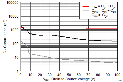
| Ciss | Input Capacitance | VGS = 0 V, VDS = 50 V, f = 1 MHz | 1290 | 1680 | pF | ||
| Coss | Output Capacitance | 257 | 330 | pF | |||
| Crss | Reverse Transfer Capacitance | 5.7 | 7.4 | pF | |||
| RG | Series Gate Resistance | 1.1 | 2.2 | Ω | |||
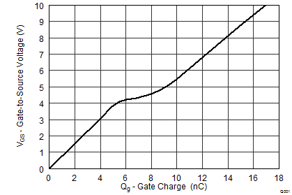
| Qg | Gate Charge Total (10 V) | VDS = 50 V, ID = 10 A | 17 | 22 | nC | ||
| Qgd | Gate Charge Gate to Drain | 3.2 | nC | ||||
| Qgs | Gate Charge Gate to Source | 5.1 | nC | ||||
| Qg(th) | Gate Charge at Vth | 3.3 | nC | ||||
| Qoss | Output Charge | VDS = 50 V, VGS = 0 V | 44 | nC | |||
| td(on) | Turn On Delay Time | VDS = 50 V, VGS = 10 V, IDS = 10 A, RG = 0 Ω |
9 | ns | |||
| tr | Rise Time | 14 | ns | ||||
| td(off) | Turn Off Delay Time | 20 | ns | ||||
| tf | Fall Time | 6 | ns | ||||
| DIODE CHARACTERISTICS | |||||||
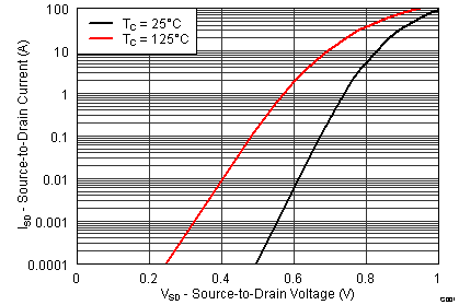
| VSD | Diode Forward Voltage | ISD = 10 A, VGS = 0 V | 0.8 | 1.0 | V | ||
| Qrr | Reverse Recovery Charge | VDS= 50 V, IF = 10 A, di/dt = 300 A/μs |
134 | nC | |||
| trr | Reverse Recovery Time | 53 | ns | ||||
5.2 Thermal Information
(TA = 25°C unless otherwise stated)| PARAMETER | MIN | TYP | MAX | UNIT | |
|---|---|---|---|---|---|
| RθJC | Junction-to-Case Thermal Resistance (1) | 2.0 | °C/W | ||
| RθJA | Junction-to-Ambient Thermal Resistance(1)(2) | 50 | |||
(1) RθJC is determined with the device mounted on a 1-inch2 (6.45-cm2), 2-oz. (0.071-mm thick) Cu pad on a 1.5-inch × 1.5-inch (3.81-cm × 3.81-cm), 0.06-inch (1.52-mm) thick FR4 PCB. RθJC is specified by design, whereas RθJA is determined by the user’s board design.
(2) Device mounted on FR4 material with 1-inch2 (6.45-cm2), 2-oz. (0.071-mm thick) Cu.
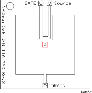 |
Max RθJA = 50°C/W when mounted on 1 inch2 (6.45 cm2) of 2-oz. (0.071-mm thick) Cu. |
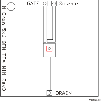 |
Max RθJA = 115°C/W when mounted on a minimum pad area of 2-oz. (0.071-mm thick) Cu. |
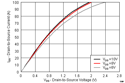
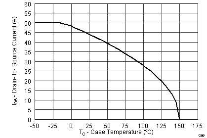
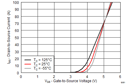
5.3 Typical MOSFET Characteristics
(TA = 25°C unless otherwise stated)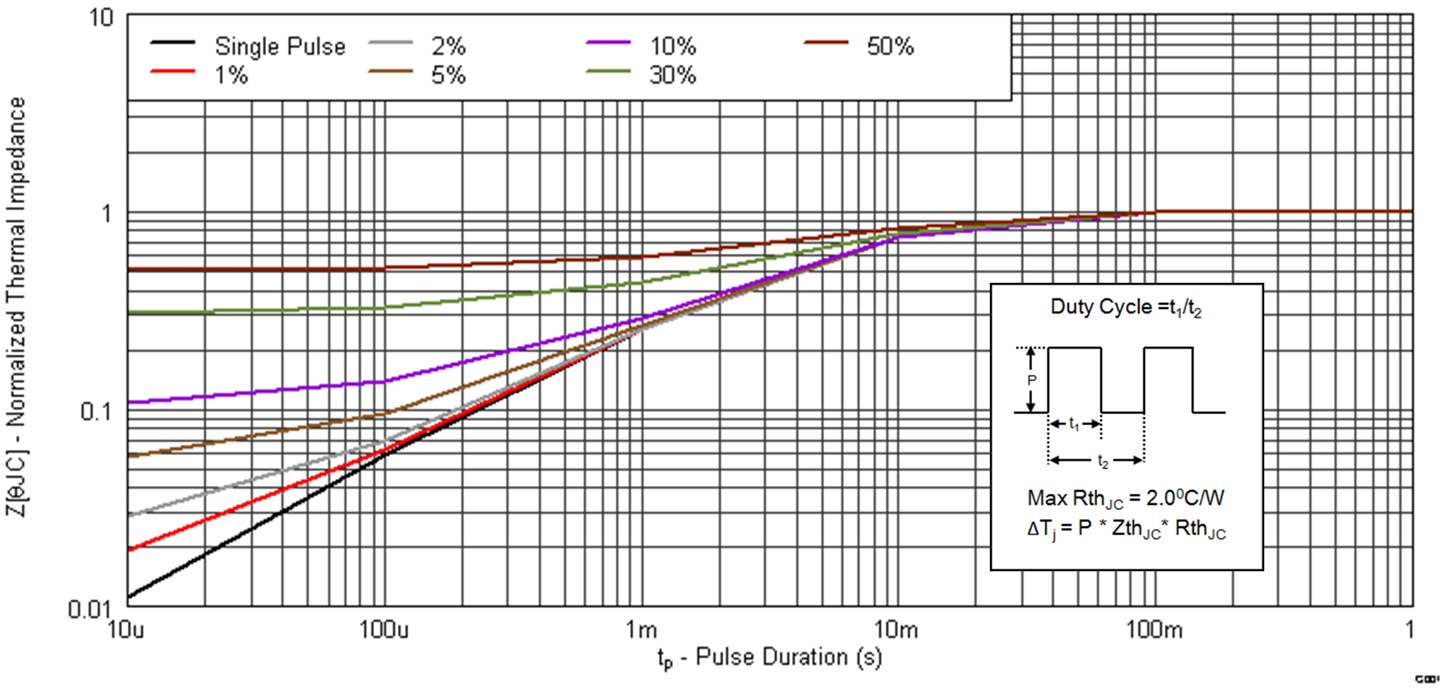
| ID = 10 A | VDS = 50 V | |
| ID = 250 µA | ||
| ID = 10 A | ||
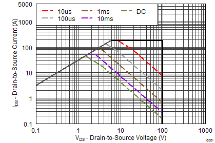
| Single Pulse | Max RθJC = 2.0°C/W | |
| VDS = 5 V | ||