ZHCSCP6A January 2014 – August 2014 CSD19501KCS
PRODUCTION DATA.
5 Specifications
5.1 Electrical Characteristics
(TA = 25°C unless otherwise stated)| PARAMETER | TEST CONDITIONS | MIN | TYP | MAX | UNIT | ||
|---|---|---|---|---|---|---|---|
| STATIC CHARACTERISTICS | |||||||
| BVDSS | Drain-to-Source Voltage | VGS = 0 V, ID = 250 μA | 80 | V | |||
| IDSS | Drain-to-Source Leakage Current | VGS = 0 V, VDS = 64 V | 1 | μA | |||
| IGSS | Gate-to-Source Leakage Current | VDS = 0 V, VGS = 20 V | 100 | nA | |||
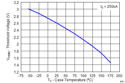
| VGS(th) | Gate-to-Source Threshold Voltage | VDS = VGS, ID = 250 μA | 2.2 | 2.6 | 3.2 | V | |
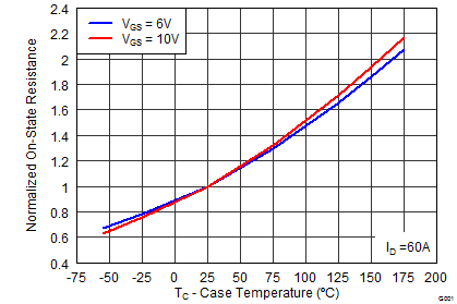
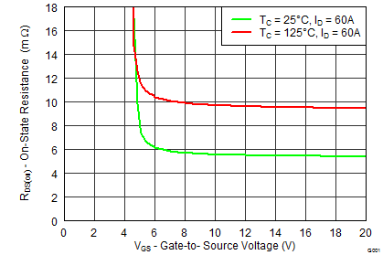
| RDS(on) | Drain-to-Source On-Resistance | VGS = 6 V, ID = 60 A | 6.2 | 7.9 | mΩ | ||
| VGS = 10 V, ID = 60 A | 5.5 | 6.6 | mΩ | ||||
| gƒs | Transconductance | VDS = 8 V, ID = 60 A | 137 | S | |||
| DYNAMIC CHARACTERISTICS | |||||||
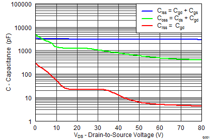
| Ciss | Input Capacitance | VGS = 0 V, VDS = 40 V, ƒ = 1 MHz | 3060 | 3980 | pF | ||
| Coss | Output Capacitance | 784 | 1020 | pF | |||
| Crss | Reverse Transfer Capacitance | 12.4 | 16.1 | pF | |||
| RG | Series Gate Resistance | 1.3 | 2.6 | Ω | |||
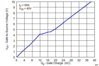
| Qg | Gate Charge Total (10 V) | VDS = 40 V, ID = 60 A | 38 | 50 | nC | ||
| Qgd | Gate Charge Gate-to-Drain | 5.8 | nC | ||||
| Qgs | Gate Charge Gate-to-Source | 12.4 | nC | ||||
| Qg(th) | Gate Charge at Vth | 7.5 | nC | ||||
| Qoss | Output Charge | VDS = 40 V, VGS = 0 V | 98 | nC | |||
| td(on) | Turn On Delay Time | VDS = 50 V, VGS = 10 V, IDS = 60 A, RG = 0 Ω |
21 | ns | |||
| tr | Rise Time | 15 | ns | ||||
| td(off) | Turn Off Delay Time | 39 | ns | ||||
| tƒ | Fall Time | 5 | ns | ||||
| DIODE CHARACTERISTICS | |||||||
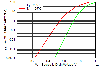
| VSD | Diode Forward Voltage | ISD = 60 A, VGS = 0 V | 0.9 | 1.1 | V | ||
| Qrr | Reverse Recovery Charge | VDS= 40 V, IF = 60 A, di/dt = 300 A/μs |
230 | nC | |||
| trr | Reverse Recovery Time | 74 | ns | ||||
5.2 Thermal Information
(TA = 25°C unless otherwise stated)| THERMAL METRIC | MIN | TYP | MAX | UNIT | |
|---|---|---|---|---|---|
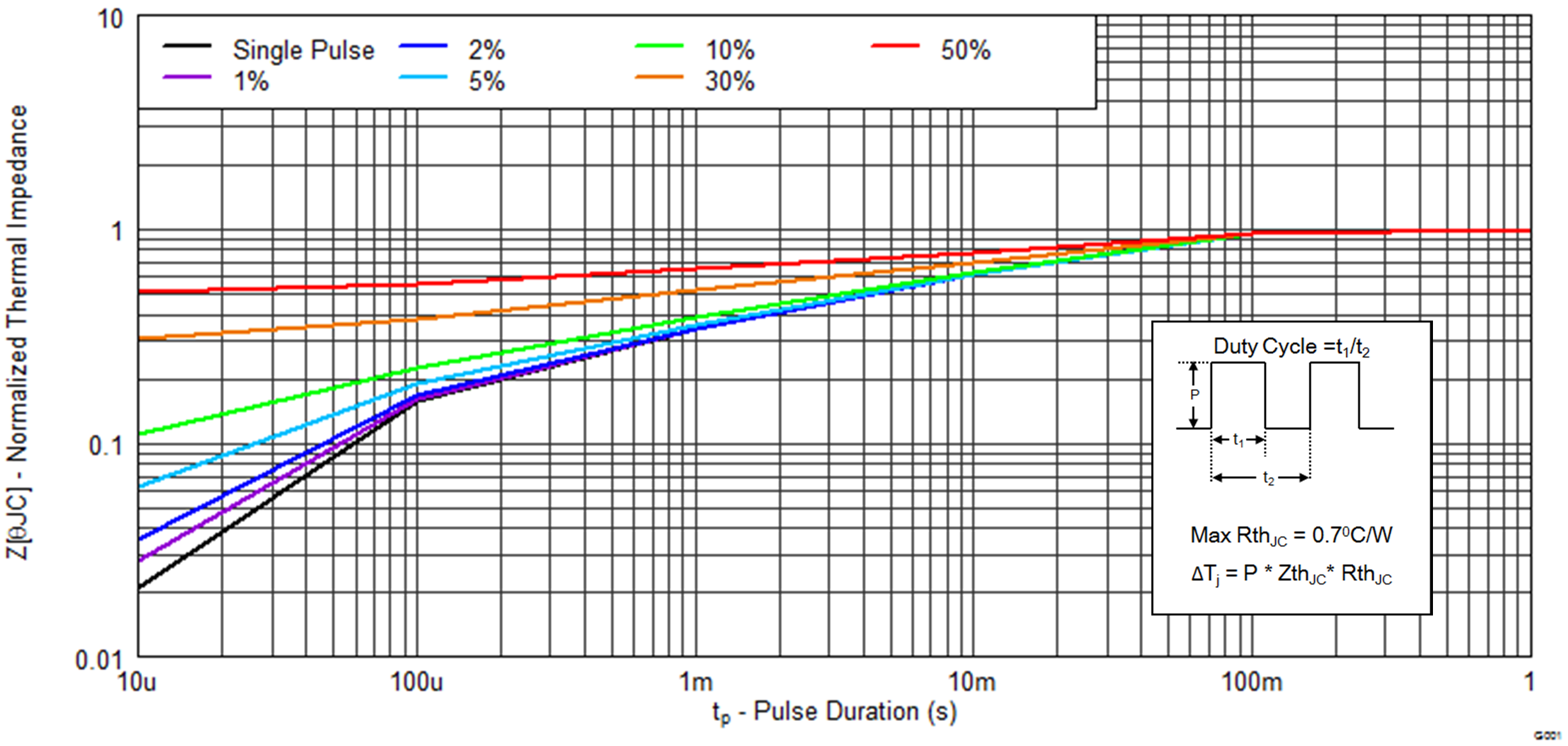
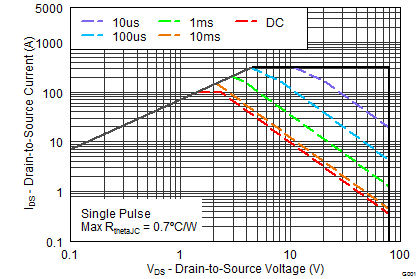
| RθJC | Junction-to-Case Thermal Resistance | 0.7 | °C/W | ||
| RθJA | Junction-to-Ambient Thermal Resistance | 62 | |||
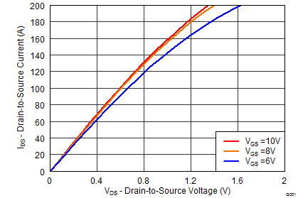
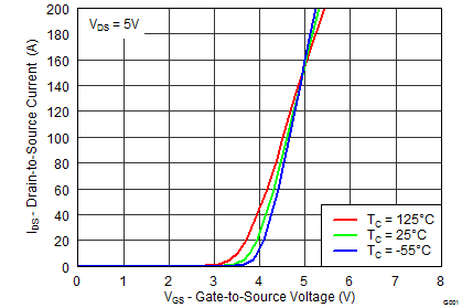
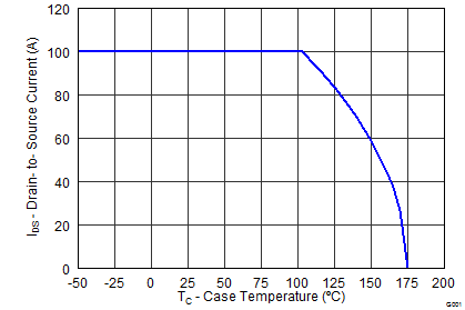
5.3 Typical MOSFET Characteristics
(TA = 25°C unless otherwise stated)