| STATIC CHARACTERISTICS |
| BVDSS |
Drain-to-Source Voltage |
VGS = 0 V, ID = 250 μA |
30 |
|
|
V |
| IDSS |
Drain-to-Source Leakage Current |
VGS = 0 V, VDS = 24 V |
|
|
1 |
μA |
| IGSS |
Gate-to-Source Leakage Current |
VDS = 0 V, VGS = ±20 V |
|
|
100 |
nA |
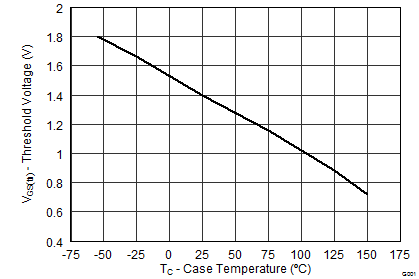
| VGS(th) |
Gate-to-Source Threshold Voltage |
VDS = VGS, ID = 250 μA |
1.1 |
1.4 |
1.8 |
V |
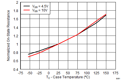
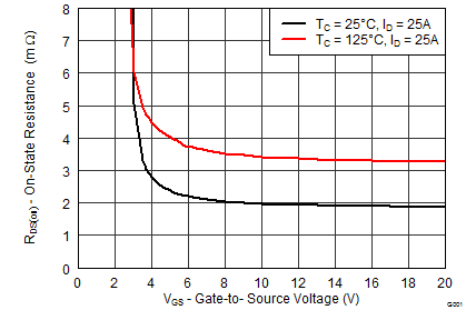
| RDS(on) |
Drain-to-Source On-Resistance |
VGS = 4.5 V, ID = 25 A |
|
2.6 |
3.2 |
mΩ |
| VGS = 10 V, ID = 25 A |
|
1.9 |
2.3 |
| gƒs |
Transconductance |
VDS = 3 V, ID = 25 A |
|
118 |
|
S |
| DYNAMIC CHARACTERISTICS |
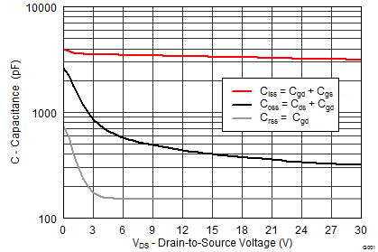
| CISS |
Input Capacitance |
VGS = 0 V, VDS = 15 V, ƒ = 1 MHz |
|
3400 |
4420 |
pF |
| COSS |
Output Capacitance |
|
393 |
511 |
pF |
| CRSS |
Reverse Transfer Capacitance |
|
157 |
204 |
pF |
| Rg |
Series Gate Resistance |
|
|
0.9 |
1.8 |
Ω |
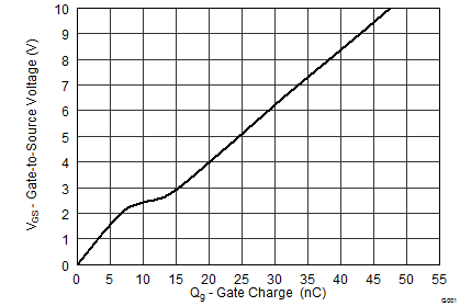
| Qg |
Gate Charge Total (4.5 V) |
VDS = 15 V, ID = 25 A |
|
23 |
30 |
nC |
| Qgd |
Gate Charge Gate-to-Drain |
|
5.4 |
|
nC |
| Qgs |
Gate Charge Gate-to-Source |
|
8.5 |
|
nC |
| Qg(th) |
Gate Charge at Vth |
|
4.6 |
|
nC |
| QOSS |
Output Charge |
VDS = 15 V, VGS = 0 V |
|
11.6 |
|
nC |
| td(on) |
Turn On Delay Time |
VDS = 15 V, VGS = 4.5 V ID = 25 A
RG = 2 Ω |
|
4 |
|
ns |
| tr |
Rise Time |
|
10 |
|
ns |
| td(off) |
Turn Off Delay Time |
|
20 |
|
ns |
| tƒ |
Fall Time |
|
3 |
|
ns |
| DIODE CHARACTERISTICS |
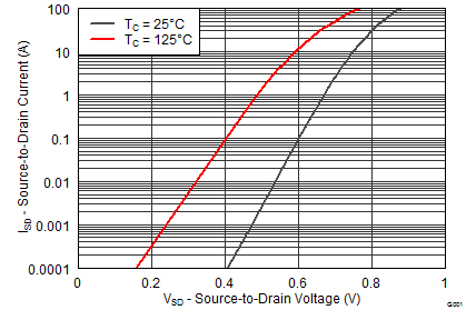
| VSD |
Diode Forward Voltage |
IS = 25 A, VGS = 0 V |
|
0.8 |
1 |
V |
| Qrr |
Reverse Recovery Charge |
VDD = 15 V, IF = 25 A, di/dt = 300 A/μs |
|
15 |
|
nC |
| trr |
Reverse Recovery Time |
|
13 |
|
ns |