SLPS247E December 2009 – August 2014 CSD16340Q3
PRODUCTION DATA.
5 Specifications
5.1 Electrical Characteristics
(TA = 25°C unless otherwise stated)| PARAMETER | TEST CONDITIONS | MIN | TYP | MAX | UNIT | ||
|---|---|---|---|---|---|---|---|
| STATIC CHARACTERISTICS | |||||||
| BVDSS | Drain-to-Source Voltage | VGS = 0 V, IDS = 250 μA | 25 | V | |||
| IDSS | Drain-to-Source Leakage Current | VGS = 0 V, VDS = 20 V | 1 | μA | |||
| IGSS | Gate-to-Source Leakage Current | VDS = 0 V, VGS = +10/–8 V | 100 | nA | |||
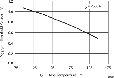
| VGS(th) | Gate-to-Source Threshold Voltage | VDS = VGS, IDS = 250 μA | 0.6 | 0.85 | 1.1 | V | |
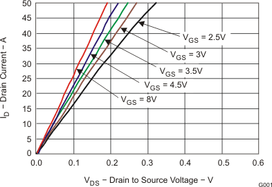
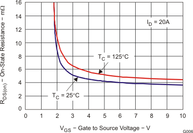
| RDS(on) | Drain-to-Source On-Resistance | VGS = 2.5 V, IDS = 20 A | 6.1 | 7.8 | mΩ | ||
| VGS = 4.5 V, IDS = 20 A | 4.3 | 5.5 | mΩ | ||||
| VGS = 8 V, IDS = 20 A | 3.8 | 4.5 | mΩ | ||||
| gƒs | Transconductance | VDS = 15 V, IDS = 20 A | 121 | S | |||
| DYNAMIC CHARACTERISTICS | |||||||
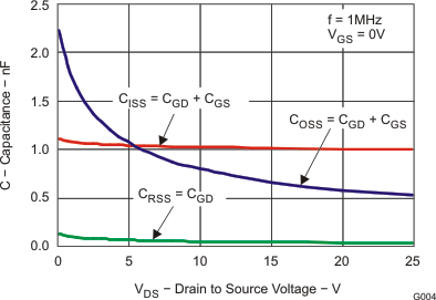
| CISS | Input Capacitance | VGS = 0 V, VDS = 12.5 V, ƒ = 1 MHz | 1050 | 1350 | pF | ||
| COSS | Output Capacitance | 730 | 950 | pF | |||
| CRSS | Reverse Transfer Capacitance | 53 | 69 | pF | |||
| Rg | Series Gate Resistance | 1.5 | 3 | Ω | |||
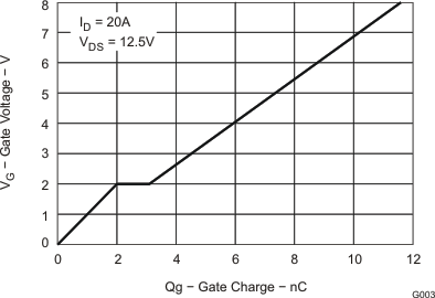
| Qg | Gate Charge Total (4.5 V) | VDS = 12.5 V, ID = 20 A | 6.5 | 9.2 | nC | ||
| Qgd | Gate Charge Gate-to-Drain | 1.2 | nC | ||||
| Qgs | Gate Charge Gate-to-Source | 2.1 | nC | ||||
| Qg(th) | Gate Charge at Vth | 1 | nC | ||||
| QOSS | Output Charge | VDS = 13 V, VGS = 0 V | 15 | nC | |||
| td(on) | Turn On Delay Time | VDS = 12.5 V, VGS = 4.5 V, ID = 20 A RG = 2 Ω |
4.8 | ns | |||
| tr | Rise Time | 16.1 | ns | ||||
| td(off) | Turn Off Delay Time | 13.8 | ns | ||||
| tƒ | Fall Time | 5.2 | ns | ||||
| DIODE CHARACTERISTICS | |||||||
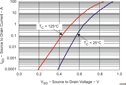
| VSD | Diode Forward Voltage | IS = 20 A, VGS = 0 V | 0.8 | 1 | V | ||
| Qrr | Reverse Recovery Charge | VDD = 13 V, IF = 20 A, di/dt = 300 A/μs | 14.5 | nC | |||
| trr | Reverse Recovery Time | 20 | ns | ||||
5.2 Thermal Information
| THERMAL METRIC(1)(2) | CSD16340Q3 | UNITS | |
|---|---|---|---|
| Q3 (8 PINS) | |||
| θJA | Junction-to-Ambient Thermal Resistance | 42.0 | °C/W |
| θJCtop | Junction-to-Case (top) Thermal Resistance | 20.6 | |
| θJB | Junction-to-Board Thermal Resistance | 8.8 | |
| ψJT | Junction-to-Top Characterization Parameter | 0.3 | |
| ψJB | Junction-to-Board Characterization Parameter | 8.7 | |
| θJCbot | Junction-to-Case (bottom) Thermal Resistance | 0.1 | |
(1) For more information about traditional and new thermal metrics, see the IC Package Thermal Metrics application report, SPRA953.
(2) For thermal estimates of this device based on PCB copper area, see the TI PCB Thermal Calculator.
 |
Max RθJA = 58°C/W when mounted on 1 inch2 of 2 oz. Cu. |
 |
Max RθJA = 162°C/W when mounted on minimum pad area of 2 oz. Cu. |
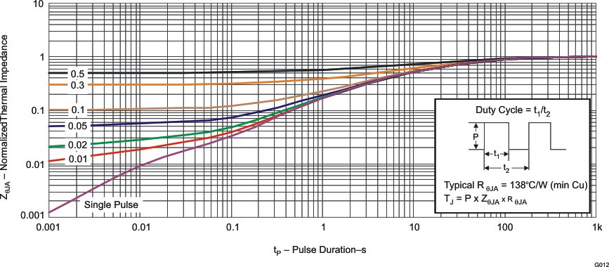
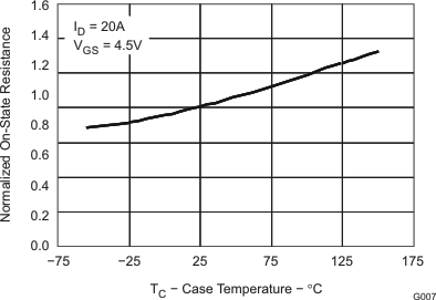
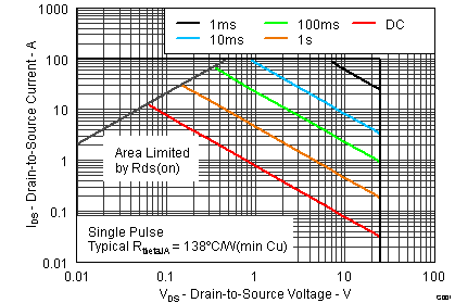
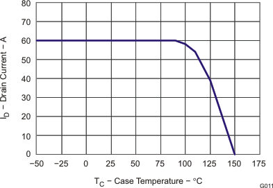
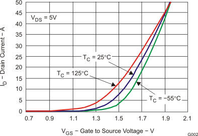
5.3 Typical MOSFET Characteristics
(TA = 25°C unless otherwise stated)