ZHCSVO9A December 1998 – March 2024 CD54AC374 , CD54ACT374 , CD74AC374 , CD74AC534 , CD74ACT374
PRODUCTION DATA
- 1
- 1 特性
- 2 说明
- 3 Pin Configuration and Functions
-
4 Specifications
- 4.1 Absolute Maximum Ratings
- 4.2 ESD Ratings
- 4.3 Recommended Operating Conditions:
- 4.4 Thermal Information
- 4.5 Electrical Characteristics: AC Series
- 4.6 Electrical Characteristics: ACT Series
- 4.7 Prerequisite for Switching: AC Series
- 4.8 Switching Characteristics: AC Series
- 4.9 Prerequisite for Switching: ACT Series
- 4.10 Switching Characteristics: ACT Series
- 5 Parameter Measurement Information
- 6 Detailed Description
- 7 Application and Implementation
- 8 Device and Documentation Support
- 9 Revision History
- 10Mechanical, Packaging, and Orderable Information
5 Parameter Measurement Information
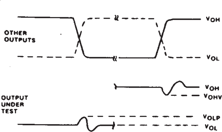
A. 1 VOHV AND VOLP ARE MEASURED WITH RESPECT TO A GROUND REFERENCE NEAR THE OUTPUT UNDER TEST.
B. INPUT PULSES HAVE THE FOLLOWING CHARACTERISTICS: PRR ≤ 1 MHz, tf = 3 ns, tf = 3 ns, SKEW 1 ns.
C. R.F. FIXTURE WITH 700-MHz DESIGN RULES REQUIRED. IC SHOULD BE SOLDERED INTO TEST BOARD ANO BYPASSED WITH 0.1 μF CAPACITOR. SCOPE ANO PROBES REQUIRE 700-MHz BANDWIDTH
D. 92CS-42406
Figure 5-1 Simultaneous Switching Transient Waveforms.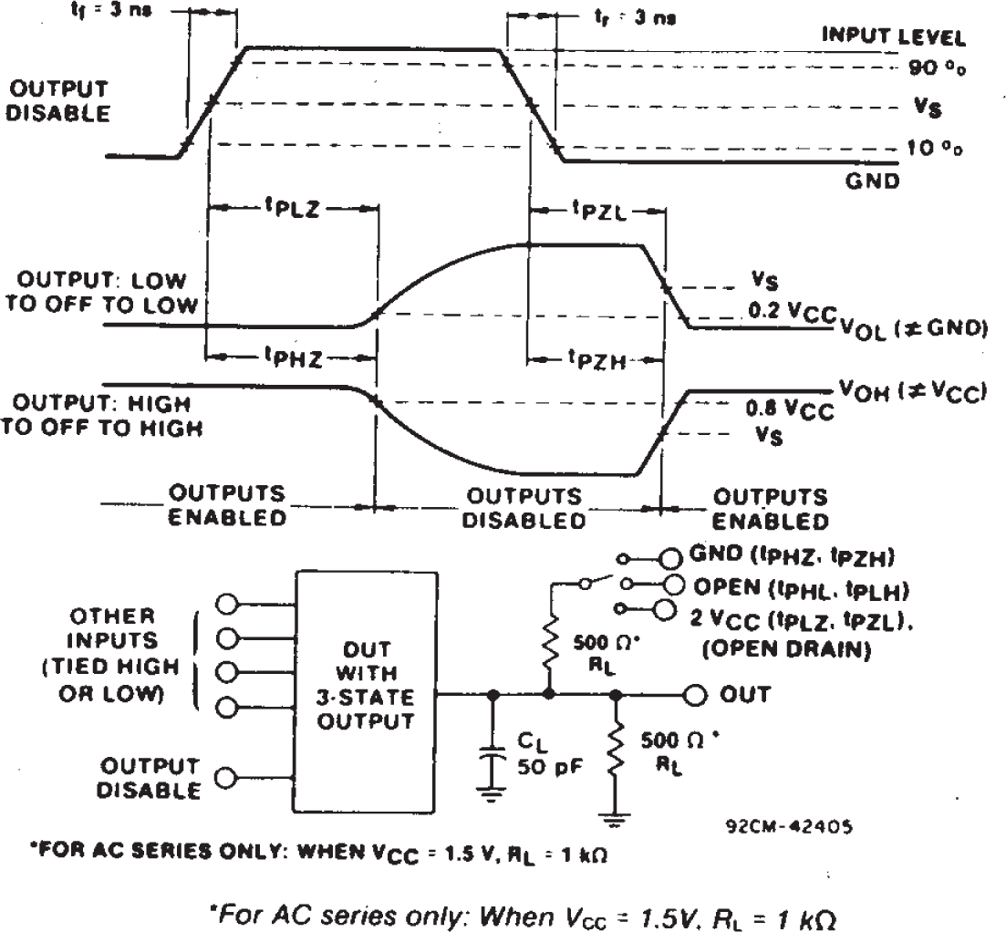 Figure 5-2 Three-state Propagation Delay Waveforms and Test Circuit.
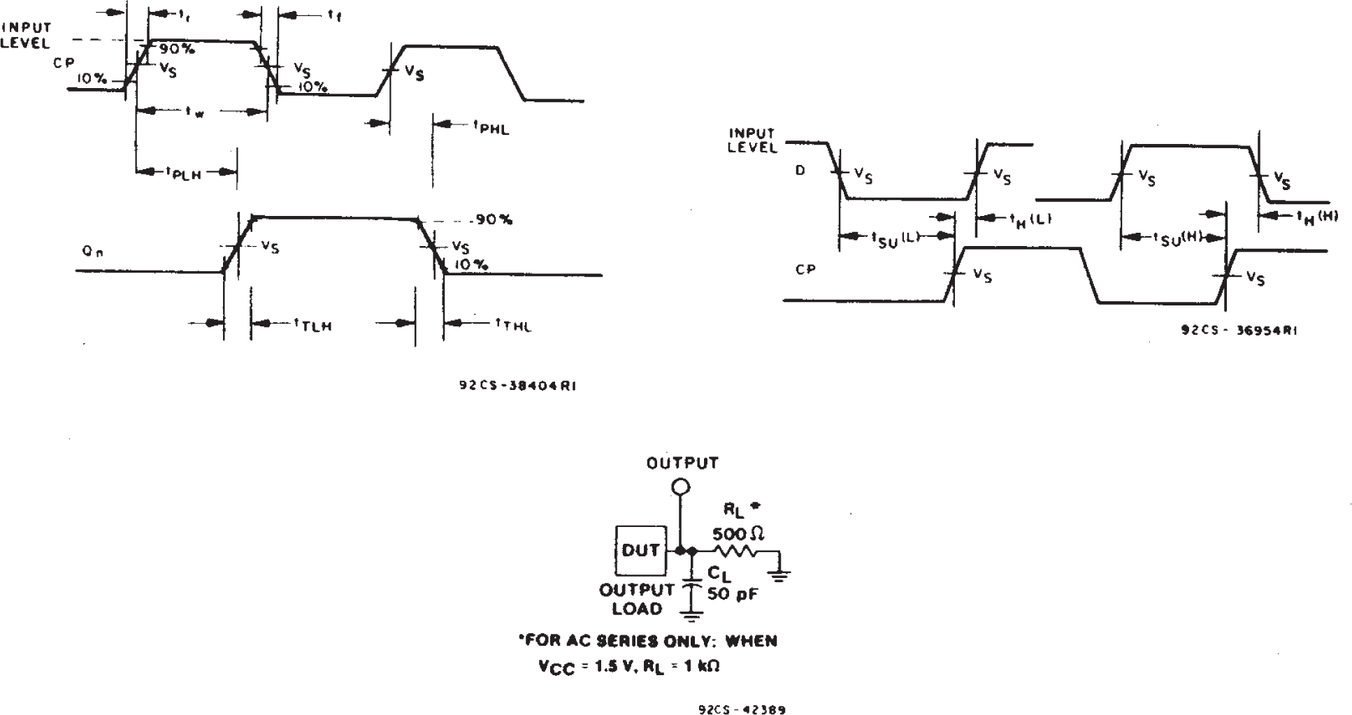 Figure 5-3 Propagation Delay Times and Test Circuit.
| CDx4AC | CDx4ACT | |
|---|---|---|
| Input Level | VCC | 3 V |
| Input Switching Voltage, VS | 0.5 VCC | 1.5 V |
| Output Switching Voltage. VS | 0.5 VCC | 0.5 VCC |