ZHCSBX5B October 2013 – October 2014 CC1201
PRODUCTION DATA.
- 1 器件概述
- 2修订历史记录
- 3Terminal Configuration and Functions
-
4Specifications
- 4.1 Absolute Maximum Ratings
- 4.2 Handling Ratings
- 4.3 Recommended Operating Conditions (General Characteristics)
- 4.4 Thermal Resistance Characteristics for RHB Package
- 4.5 RF Characteristics
- 4.6 Regulatory Standards
- 4.7 Current Consumption, Static Modes
- 4.8 Current Consumption, Transmit Modes
- 4.9 Current Consumption, Receive Modes
- 4.10
Receive Parameters
- 4.10.1 General Receive Parameters (High-Performance Mode)
- 4.10.2 RX Performance in 868-, 915-, and 920-MHz Bands (High-Performance Mode)
- 4.10.3 RX Performance in 433-MHz Band (High-Performance Mode)
- 4.10.4 RX Performance in 169-MHz Band (High-Performance Mode)
- 4.10.5 RX Performance in Low-Power Mode
- 4.11 Transmit Parameters
- 4.12 PLL Parameters
- 4.13 Wake-up and Timing
- 4.14 40-MHz Crystal Oscillator
- 4.15 40-MHz Clock Input (TCXO)data to TCXO table
- 4.16 32-kHz Clock Input
- 4.17 40-kHz RC Oscillator
- 4.18 I/O and Reset
- 4.19 Temperature Sensor
- 4.20 Typical Characteristics
- 5Detailed Description
- 6Typical Application Circuit
- 7器件和文档支持
- 8机械封装和可订购信息
封装选项
请参考 PDF 数据表获取器件具体的封装图。
机械数据 (封装 | 引脚)
- RHB|32
散热焊盘机械数据 (封装 | 引脚)
- RHB|32
订购信息
5 Detailed Description
5.1 Block Diagram
Figure 5-1 shows the system block diagram of the CC120x family of devices.
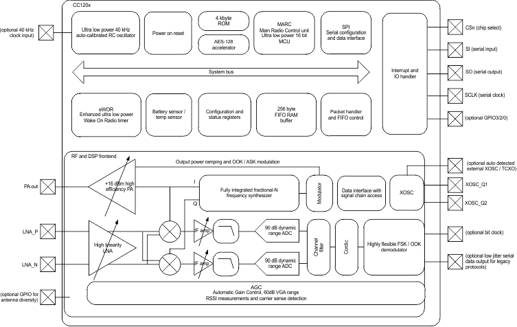 Figure 5-1 System Block Diagram
5.2 Frequency Synthesizer
At the center of the CC1201 device there is a fully integrated, fractional-N, ultra-high-performance frequency synthesizer. The frequency synthesizer is designed for excellent phase noise performance, providing very high selectivity and blocking performance. The system is designed to comply with the most stringent regulatory spectral masks at maximum transmit power.
Either a crystal can be connected to XOSC_Q1 and XOSC_Q2, or a TCXO can be connected to the EXT_XOSC input. The oscillator generates the reference frequency for the synthesizer, as well as clocks for the analog-to-digital converter (ADC) and the digital part. To reduce system cost, the CC1201 device has high-accuracy frequency estimation and compensation registers to measure and compensate for crystal inaccuracies. This compensation enables the use of lower cost crystals. If a TCXO is used, the CC1201 device automatically turns on and off the TCXO when needed to support low-power modes and Wake-On-Radio operation.
5.3 Receiver
The CC1201 device features a highly flexible receiver. The received RF signal is amplified by the low-noise amplifier (LNA) and is down-converted in quadrature (I/Q) to the intermediate frequency (IF). At IF, the I/Q signals are digitized by the high dynamic-range ADCs.
An advanced automatic gain control (AGC) unit adjusts the front-end gain, and enables the CC1201 device to receive strong and weak signals, even in the presence of strong interferers. High-attenuation channel and data filtering enable reception with strong neighbor channel interferers. The I/Q signal is converted to a phase and magnitude signal to support the FSK and OOK modulation schemes.
NOTE
A unique I/Q compensation algorithm removes any problem of I/Q mismatch, thus avoiding time-consuming and costly I/Q image calibration steps.
5.4 Transmitter
The CC1201 transmitter is based on direct synthesis of the RF frequency (in-loop modulation). To use the spectrum effectively, the CC1201 device has extensive data filtering and shaping in TX mode to support high throughput data communication in narrowband channels. The modulator also controls power ramping to remove issues such as spectral splattering when driving external high-power RF amplifiers.
5.5 Radio Control and User Interface
The CC1201 digital control system is built around the main radio control (MARC), which is implemented using an internal high-performance, 16-bit ultra-low-power processor. MARC handles power modes, radio sequencing, and protocol timing.
A 4-wire SPI serial interface is used for configuration, strobe commands, and FIFO access. The digital baseband includes support for channel configuration, packet handling, and data buffering. The host MCU can stay in sleep mode until a valid RF packet is received. This greatly reduces power consumption. When the host MCU receives a valid RF packet, it burst-reads the data. This reduces the required computing power.
The CC1201 radio control and user interface are based on the widely used CC1101 transceiver. This relationship enables an easy transition between the two platforms. The command strobes and the main radio states are the same for the two platforms.
For legacy formats, the CC1201 device also supports two serial modes.
- Synchronous serial mode: The CC1201 device performs bit synchronization and provides the MCU with a bit clock with associated data.
- Transparent mode: The CC1201 device outputs the digital baseband signal using a digital interpolation filter to eliminate jitter introduced by digital filtering and demodulation.
5.6 Enhanced Wake-On-Radio (eWOR)
eWOR, using a flexible integrated sleep timer, enables automatic receiver polling with no intervention from the MCU. When the CC1201 device enters RX mode, it listens and then returns to sleep if a valid RF packet is not received. The sleep interval and duty cycle can be configured to make a trade-off between network latency and power consumption. Incoming messages are time-stamped to simplify timer re-synchronization.
The eWOR timer runs off an ultra-low-power RC oscillator. To improve timing accuracy, the RC oscillator can be automatically calibrated to the RF crystal in configurable intervals.
5.7 RX Sniff Mode
The CC1201 device supports quick start up times, and requires few preamble bits. RX Sniff Mode uses these conditions to dramatically reduce the current consumption while the receiver is waiting for data.
Because the CC1201 device can wake up and settle much faster than the duration of most preambles, it is not required to be in RX mode continuously while waiting for a packet to arrive. Instead, the Enhanced Wake On Radio feature can be used to put the device into sleep mode periodically. By setting an appropriate sleep time, the CC1201 device can wake up and receive the packet when it arrives with no performance loss. This sequence removes the need for accurate timing synchronization between transmitter and receiver, and lets the user trade off current consumption between the transmitter and receiver.
For more information, see the sniff mode design note (SWRA428).
5.8 Antenna Diversity
Antenna diversity can increase performance in a multipath environment. An external antenna switch is required. The CC1201 device uses one of the GPIO pins to automatically control the switch. This device also supports differential output control signals typically used in RF switches.
If antenna diversity is enabled, the GPIO alternates between high and low states until a valid RF input signal is detected. An optional acknowledge packet can be transmitted without changing the state of the GPIO.
An incoming RF signal can be validated by received signal strength or by using the automatic preamble detector. Using the automatic preamble detector ensures a more robust system and avoids the need to set a defined signal strength threshold (such a threshold sets the sensitivity limit of the system).
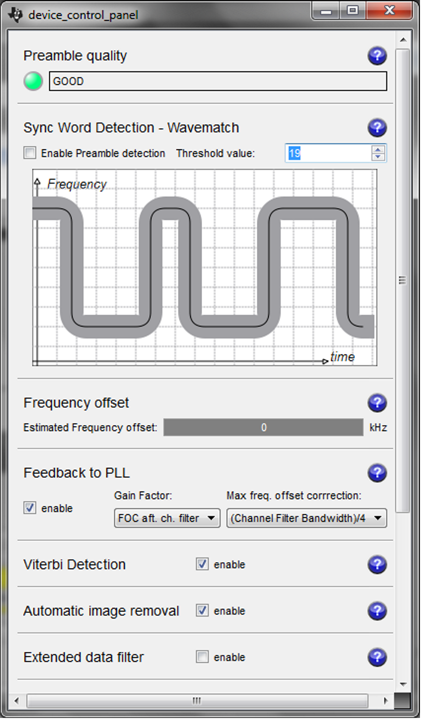
5.9 WaveMatch
Advanced capture logic locks onto the synchronization word and does not require preamble settling bytes. Therefore, receiver settling time is reduced to the settling time of the AGC, typically 4 bits.
The WaveMatch feature also greatly reduces false sync triggering on noise, further reducing the power consumption and improving sensitivity and reliability. The same logic can also be used as a high-performance preamble detector to reliably detect a valid preamble in the channel.