ZHCSBX5B October 2013 – October 2014 CC1201
PRODUCTION DATA.
- 1 器件概述
- 2修订历史记录
- 3Terminal Configuration and Functions
-
4Specifications
- 4.1 Absolute Maximum Ratings
- 4.2 Handling Ratings
- 4.3 Recommended Operating Conditions (General Characteristics)
- 4.4 Thermal Resistance Characteristics for RHB Package
- 4.5 RF Characteristics
- 4.6 Regulatory Standards
- 4.7 Current Consumption, Static Modes
- 4.8 Current Consumption, Transmit Modes
- 4.9 Current Consumption, Receive Modes
- 4.10
Receive Parameters
- 4.10.1 General Receive Parameters (High-Performance Mode)
- 4.10.2 RX Performance in 868-, 915-, and 920-MHz Bands (High-Performance Mode)
- 4.10.3 RX Performance in 433-MHz Band (High-Performance Mode)
- 4.10.4 RX Performance in 169-MHz Band (High-Performance Mode)
- 4.10.5 RX Performance in Low-Power Mode
- 4.11 Transmit Parameters
- 4.12 PLL Parameters
- 4.13 Wake-up and Timing
- 4.14 40-MHz Crystal Oscillator
- 4.15 40-MHz Clock Input (TCXO)data to TCXO table
- 4.16 32-kHz Clock Input
- 4.17 40-kHz RC Oscillator
- 4.18 I/O and Reset
- 4.19 Temperature Sensor
- 4.20 Typical Characteristics
- 5Detailed Description
- 6Typical Application Circuit
- 7器件和文档支持
- 8机械封装和可订购信息
封装选项
请参考 PDF 数据表获取器件具体的封装图。
机械数据 (封装 | 引脚)
- RHB|32
散热焊盘机械数据 (封装 | 引脚)
- RHB|32
订购信息
4 Specifications
All measurements performed on CC1200EM_868_930 rev.1.0.0, CC1200EM_420_470 rev.1.0.1, or CC1200EM_169 rev.1.2.
4.1 Absolute Maximum Ratings(1)(2)
over operating free-air temperature range (unless otherwise noted)| PARAMETER | MIN | MAX | UNIT | CONDITION | |
|---|---|---|---|---|---|
| Supply voltage (VDD, AVDD_x) | –0.3 | 3.9 | V | All supply pins must have the same voltage | |
| Input RF level | +10 | dBm | |||
| Voltage on any digital pin | –0.3 | VDD+0.3 | V | max 3.9 V | |
| Voltage on any analog Pin (including DCPL pins) |
–0.3 | 2.0 | V | ||
4.2 Handling Ratings
| MIN | MAX | UNIT | ||||
|---|---|---|---|---|---|---|
| Tstg | Storage temperature range | –40 | 125 | °C | ||
| VESD | Electrostatic discharge (ESD) performance: | Human body model (HBM), per ANSI/ESDA/JEDEC JS001(1) | –2 | 2 | kV | |
| Charged device model (CDM), per JESD22-C101(2) | All pins | –500 | 500 | V | ||
4.3 Recommended Operating Conditions (General Characteristics)
| PARAMETER | MIN | TYP | MAX | UNIT | CONDITION | |
|---|---|---|---|---|---|---|
| Voltage supply range | 2.0 | 3.6 | V | All supply pins must have the same voltage | ||
| Voltage on digital inputs | 0 | VDD | V | |||
| Temperature range | –40 | 85 | °C | Ambient | ||
4.4 Thermal Resistance Characteristics for RHB Package
| °C/W(1) | AIR FLOW (m/s)(2) | ||
|---|---|---|---|
| RθJC | Junction-to-case (top) | 21.1 | 0.00 |
| RθJB | Junction-to-board | 5.3 | 0.00 |
| RθJA | Junction-to-free air | 31.3 | 0.00 |
| PsiJT | Junction-to-package top | 0.2 | 0.00 |
| PsiJB | Junction-to-board | 5.3 | 0.00 |
| RθJC | Junction-to-case (bottom) | 0.8 | 0.00 |
- JESD51-2, Integrated Circuits Thermal Test Method Environmental Conditions - Natural Convection (Still Air)
- JESD51-3, Low Effective Thermal Conductivity Test Board for Leaded Surface Mount Packages
- JESD51-7, High Effective Thermal Conductivity Test Board for Leaded Surface Mount Packages
- JESD51-9, Test Boards for Area Array Surface Mount Package Thermal Measurements
4.5 RF Characteristics
| PARAMETER | MIN | TYP | MAX | UNIT | CONDITION | |
|---|---|---|---|---|---|---|
| Frequency bands | 820 | 950 | MHz | |||
| 410 | 475 | MHz | ||||
| 164 | 190 | MHz | ||||
| (274) | (316.6) | MHz | Contact TI for more information about the use of these frequency bands. | |||
| (205) | (237.5) | MHz | ||||
| (137) | (158.3) | MHz | ||||
| Frequency resolution | 30 | Hz | In 820–950 MHz band | |||
| 15 | Hz | In 410–475 MHz band | ||||
| 6 | Hz | In 164–190 MHz band | ||||
| Data rate | 0 | 1250 | kbps | Packet mode | ||
| 0 | 625 | kbps | Transparent mode | |||
4.6 Regulatory Standards
| PERFORMANCE MODE | FREQUENCY BAND | SUITABLE FOR COMPLIANCE WITH | COMMENTS | |
|---|---|---|---|---|
| High-performance mode | 820–950 MHz | ARIB STD-T108 ETSI EN 300 220 receiver categories 2 and 3 FCC PART 15.247 FCC PART 15.249 |
Performance also suitable for systems targeting maximum allowed output power in the respective bands, using a range extender such as the CC1190 | |
| 410–475 MHz | ETSI EN 300 220 receiver categories 2 and 3 | Performance also suitable for systems targeting maximum allowed output power in the respective bands, using a range extender | ||
| 164–190 MHz | ETSI EN 300 220 | Performance also suitable for systems targeting maximum allowed output power in the respective bands, using a range extender | ||
| Low-power mode | 820–950 MHz | ETSI EN 300 220 receiver categories 2 and 3 FCC PART 15.247 FCC PART 15.249 |
||
| 410–475 MHz | ETSI EN 300 220 receiver categories 2 and 3 | |||
| 164–190 MHz | ETSI EN 300 220 | |||
4.7 Current Consumption, Static Modes
TA = 25°C, VDD = 3.0 V (unless otherwise noted)| PARAMETER | MIN | TYP | MAX | UNIT | CONDITION | |
|---|---|---|---|---|---|---|
| Power down with retention | 0.12 | 1 | µA | |||
| 0.5 | µA | Low-power RC oscillator running | ||||
| XOFF mode | 180 | µA | Crystal oscillator / TCXO disabled | |||
| IDLE mode | 1.5 | mA | Clock running, system waiting with no radio activity | |||
4.8 Current Consumption, Transmit Modes
4.8.1 868-, 915-, and 920-MHz Bands (High-Performance Mode)
TA = 25°C, VDD = 3.0 V (unless otherwise noted)
| PARAMETER | MIN | TYP | MAX | UNIT | CONDITION | |
|---|---|---|---|---|---|---|
| TX current consumption +14 dBm | 46 | mA | ||||
| TX current consumption +10 dBm | 36 | mA | ||||
4.8.2 433-MHz Band (High-Performance Mode)
TA = 25°C, VDD = 3.0 V (unless otherwise noted)
| PARAMETER | MIN | TYP | MAX | UNIT | CONDITION | |
|---|---|---|---|---|---|---|
| TX current consumption +15 dBm | 49 | mA | ||||
| TX current consumption +14 dBm | 46 | mA | ||||
| TX current consumption +10 dBm | 35 | mA | ||||
4.8.3 169-MHz Band (High Performance Mode)
TA = 25°C, VDD = 3.0 V (unless otherwise noted)
| PARAMETER | MIN | TYP | MAX | UNIT | CONDITION | |
|---|---|---|---|---|---|---|
| TX current consumption +15 dBm | 54 | mA | ||||
| TX current consumption +14 dBm | 50 | mA | ||||
| TX current consumption +10 dBm | 39 | mA | ||||
4.8.4 Low-Power Mode
TA = 25°C, VDD = 3.0 V, fc = 869.5 MHz (unless otherwise noted)
| PARAMETER | MIN | TYP | MAX | UNIT | CONDITION | |
|---|---|---|---|---|---|---|
| TX Current Consumption +10 dBm | 33.6 | mA | ||||
4.9 Current Consumption, Receive Modes
4.9.1 High-Performance Mode
TA = 25°C, VDD = 3.0 V, fc = 869.5 MHz (unless otherwise noted)
| PARAMETER | MIN | TYP | MAX | UNIT | CONDITION | |
|---|---|---|---|---|---|---|
| RX wait for sync | Using RX Sniff Mode, where the receiver wakes up at regular intervals looking for an incoming packet. Sniff mode configured to terminate on carrier sense, and is measured using RSSI_VALID _COUNT = 1 (0 for 1.2 kbps), AGC_WIN_SIZE = 0, and SETTLE_WAIT = 1.(1) |
|||||
| 1.2 kbps, 4-byte preamble | 0.5 | mA | ||||
| 38.4 kbps, 12-byte preamble | 3.5 | mA | ||||
| 50 kbps, 24-byte preamble | 2.1 | mA | ||||
| RX peak current | Peak current consumption during packet reception | |||||
| 1.2 kbps | 23.6 | mA | ||||
| Average current consumption Check for data packet every 1 second using eWOR |
8 | µA | 50 kbps, 5-byte preamble, 40-kHz RC oscillator used as eWOR timer | |||
4.9.2 Low-Power Mode
TA = 25°C, VDD = 3.0 V, fc = 869.5 MHz (unless otherwise noted)
| PARAMETER | MIN | TYP | MAX | UNIT | CONDITION | |
|---|---|---|---|---|---|---|
| RX Peak current low-power RX mode | Peak current consumption during packet reception at the sensitivity limit | |||||
| 50 kbps | 19 | mA | ||||
4.10 Receive Parameters
All RX measurements made at the antenna connector, to a bit error rate (BER) limit of 1%. Selectivity and blocking is measured with the desired signal 3 dB above the sensitivity level.
4.10.1 General Receive Parameters (High-Performance Mode)
TA = 25°C, VDD = 3.0 V, fc = 869.5 MHz (unless otherwise noted)
| PARAMETER | MIN | TYP | MAX | UNIT | CONDITION | |
|---|---|---|---|---|---|---|
| Saturation | +10 | dBm | ||||
| Digital channel filter programmable bandwidth | 50 | 1600 | kHz | |||
| IIP3 | –14 | dBm | At maximum gain | |||
| Data rate offset tolerance | ±14 | % | With carrier sense detection enabled | |||
| ±1600 | ppm | With carrier sense detection disabled | ||||
| Spurious emissions | Radiated emissions measured according to ETSI EN 300 220, fc = 869.5 MHz | |||||
| 1–13 GHz (VCO leakage at 3.5 GHz) | < –56 | dBm | ||||
| 30 MHz to 1 GHz | < –57 | dBm | ||||
| Optimum source impedance | (Differential or Single-Ended RX Configurations) | |||||
| 868-, 915-, and 920-MHz bands | 60 + j60 / 30 + j30 | Ω | ||||
| 433-MHz band | 100 + j60 / 50 + j30 | Ω | ||||
| 169-MHz band | 140 + j40 / 70 + j20 | Ω | ||||
4.10.2 RX Performance in 868-, 915-, and 920-MHz Bands (High-Performance Mode)
TA = 25°C, VDD = 3.0 V (unless otherwise noted)
| PARAMETER | MIN | TYP | MAX | UNIT | CONDITION |
|---|---|---|---|---|---|
| Sensitivity | –119 | dBm | 1.2 kbps 2-FSK, DEV=20 kHz CHF=50 kHz(1) | ||
| –113 | dBm | 4.8 kbps OOK CHF=128 kHz(1) | |||
| –108 | dBm | 32.768 kbps 2-GFSK, DEV=50 kHz CHF=208 kHz(1) | |||
| –110 | dBm | 38.4 kbps 2-GFSK, DEV=20 kHz CHF=104 kHz(1) | |||
| –109 | dBm | 50 kbps 2-GFSK, DEV=25 kHz, CHF=104 kHz(1) | |||
| –97 | dBm | 500 kbps 2-GMSK, CHF=833 kHz(1) | |||
| –97 | dBm | 1 Mbps 4-GFSK, DEV=400 kHz, CHF=1.66 MHz(1) | |||
| Blocking and selectivity 1.2-kbps 2-FSK, 50-kHz channel separation, 20-kHz deviation, 50-kHz channel filter |
50 | dB | ± 50 kHz (adjacent channel) | ||
| 50 | dB | ± 100 kHz (alternate channel) | |||
| 75 | dB | ± 2 MHz | |||
| 80 | dB | ± 10 MHz | |||
| Blocking and selectivity 32.768-kbps 2-GFSK, 200-kHz channel separation, 50-kHz deviation, 208-kHz channel filter |
38 | dB | ± 200 kHz | ||
| 46 | dB | ± 400 kHz | |||
| 66 | dB | ± 2 MHz | |||
| 70 | dB | ± 10 MHz | |||
| Blocking and selectivity 38.4-kbps 2-GFSK, 100-kHz channel separation, 20-kHz deviation, 104-kHz channel filter |
44 | dB | + 100 kHz (adjacent channel) | ||
| 44 | dB | ± 200 kHz (alternate channel) | |||
| 64 | dB | ± 2 MHz | |||
| 72 | dB | ± 10 MHz | |||
| Blocking and selectivity 50-kbps 2-GFSK, 200-kHz channel separation, 25-kHz deviation, 104-kHz channel filter (Same modulation format as 802.15.4g Mandatory Mode) |
41 | dB | ± 200 kHz (adjacent channel) | ||
| 46 | dB | ± 400 kHz (alternate channel) | |||
| 65 | dB | ± 2 MHz | |||
| 71 | dB | ± 10 MHz | |||
| Blocking and selectivity 100-kbps 2-GFSK, 50-kHz deviation, 208-kHz channel filter |
45 | dB | ± 400 kHz (adjacent channel) | ||
| 54 | dB | ± 800 kHz (alternate channel) | |||
| 63 | dB | ± 2 MHz | |||
| 68 | dB | ± 10 MHz | |||
| Blocking and selectivity 500-kbps GMSK, 833-kHz channel filter |
42 | dB | + 1 MHz (adjacent channel) | ||
| 42 | dB | ± 2 MHz (alternate channel) | |||
| 57 | dB | ± 10 MHz | |||
| Blocking and selectivity 1-Mbps 4-GFSK, 400-kHz deviation, 1.6-MHz channel filter |
46 | dB | ± 2 MHz (adjacent channel) | ||
| 52 | dB | ± 4 MHz (alternate channel) | |||
| 59 | dB | ± 10 MHz |
4.10.3 RX Performance in 433-MHz Band (High-Performance Mode)
TA = 25°C, VDD = 3.0 V (unless otherwise noted)
| PARAMETER | MIN | TYP | MAX | UNIT | CONDITION |
|---|---|---|---|---|---|
| Sensitivity | –120 | dBm | 1.2 kbps 2-FSK, DEV=20 kHz CHF=50 kHz(1) |
||
| –111 | dBm | 38.4 kbps 2-GFSK, DEV=20 kHz CHF=104 kHz(1) | |||
| Blocking and selectivity 1.2-kbps 2-FSK, 50-kHz channel separation, 20-kHz deviation, 50-kHz channel filter |
56 | dB | ± 50 kHz (adjacent channel) | ||
| 56 | dB | ± 100 kHz (alternate channel) | |||
| 79 | dB | ± 2 MHz | |||
| 84 | dB | ± 10 MHz | |||
| Blocking and selectivity 38.4-kbps 2-GFSK, 100-kHz channel separation, 20-kHz deviation, 104-kHz channel filter |
49 | dB | + 100 kHz (adjacent channel) | ||
| 48 | dB | ± 200 kHz (alternate channel) | |||
| 66 | dB | ± 2 MHz | |||
| 74 | dB | ± 10 MHz |
4.10.4 RX Performance in 169-MHz Band (High-Performance Mode)
TA = 25°C, VDD = 3.0 V (unless otherwise noted)
| PARAMETER | MIN | TYP | MAX | UNIT | CONDITION |
|---|---|---|---|---|---|
| Sensitivity | –119 | dBm | 1.2 kbps 2-FSK, DEV=20 kHz CHF=50 kHz(1) | ||
| Blocking and Selectivity 1.2 kbps 2-FSK, 50 kHz channel separation, 20 kHz deviation, 50 kHz channel filter |
62 | dB | ± 50 kHz (adjacent channel) | ||
| 62 | dB | ± 100 kHz (alternate channel) | |||
| 81 | dB | ± 2 MHz | |||
| 85 | dB | ± 10 MHz | |||
| Image rejection (Image compensation enabled) |
67 | dB | 1.2 kbps, DEV=20 kHz, CHF=50 kHz, image at –417 kHz(1) |
4.10.5 RX Performance in Low-Power Mode
TA = 25°C, VDD = 3.0 V, fc = 869.5 MHz (unless otherwise noted)
| PARAMETER | MIN | TYP | MAX | UNIT | CONDITION |
|---|---|---|---|---|---|
| Sensitivity | –96 | dBm | 50 kbps 2-GFSK, DEV=25 kHz, CHF=119 kHz(1) | ||
| Blocking and selectivity 50 kbps 2-GFSK, 200-kHz channel separation, 25-kHz deviation, 104-kHz channel filter (Same modulation format as 802.15.4g Mandatory Mode) |
41 | dB | + 200 kHz (adjacent channel) | ||
| 45 | dB | + 400 kHz (alternate channel) | |||
| 62 | dB | ± 2 MHz | |||
| 60 | dB | ± 10 MHz | |||
| Saturation | 10 | dBm |
4.11 Transmit Parameters
TA = 25°C, VDD = 3.0 V, fc = 869.5 MHz (unless otherwise noted)
| PARAMETER | MIN | TYP | MAX | UNIT | CONDITION |
|---|---|---|---|---|---|
| Max output power | +14 | dBm | At 915/920 MHz | ||
| +15 | dBm | At 915/920 MHz with VDD = 3.6 V | |||
| +15 | dBm | At 868 MHz | |||
| +16 | dBm | At 868 MHz with VDD = 3.6 V | |||
| +15 | dBm | At 433 MHz | |||
| +16 | dBm | At 433 MHz with VDD = 3.6 V | |||
| +15 | dBm | At 169 MHz | |||
| +16 | dBm | At 169 MHz with VDD = 3.6 V | |||
| Min output power | –12 | dBm | Within fine step size range | ||
| –38 | dBm | Within coarse step size range | |||
| Output power step size | 0.4 | dB | Within fine step size range | ||
| Adjacent channel power | –60 | dBc | 4-GFSK 9.6 kbps in 12.5 kHz channel, measured in 8.75 kHz bandwidth (ETSI 300 220 compliant) | ||
| Spurious emissions (Excluding harmonics) |
Transmission at +14 dBm Suitable for systems targeting compliance with ETSI EN 300-220, FCC part 15, ARIB STD-T108 Measured in 1 MHz bandwidth |
||||
| 30 MHz–1 GHz | < –57 | dBm | |||
| 1–12.75 GHz | < –50 | dBm | |||
| Harmonics | Transmission at +14 dBm (or maximum allowed in applicable band where this is less than +14 dBm) using TI reference design Suitable for systems targeting compliance with ETSI EN 300-220, FCC part 15, ARIB STD-T108 |
||||
| Second Harm, 169 MHz (ETSI) | –43 | dBm | |||
| Third Harm, 169 MHz (ETSI) | –57 | dBm | |||
| Fourth Harm, 169 MHz (ETSI) | –63 | dBm | |||
| Second Harm, 433 MHz (ETSI) | –59 | dBm | |||
| Third Harm, 433 MHz (ETSI) | –51 | dBm | |||
| Fourth Harm, 433 MHz (ETSI) | –63 | dBm | |||
| Second Harm, 868 MHz (ETSI) | –50 | dBm | |||
| Third Harm, 868 MHz (ETSI) | –44 | dBm | |||
| Fourth Harm, 868 MHz (ETSI) | –56 | dBm | |||
| Second Harm, 915 MHz (FCC) | –58 | dBm | |||
| Third Harm, 915 MHz (FCC) | –46 | dBm | |||
| Fourth Harm, 915 MHz (FCC) | –62 | dBm | |||
| Second Harm, 920 MHz (ARIB) | –65 | dBm | |||
| Third Harm, 920 MHz (ARIB) | –60 | dBm | |||
| Optimum load impedance | |||||
| 868-, 915-, and 920-MHz bands | 35 + j35 | Ω | |||
| 433-MHz band | 55 + j25 | Ω | |||
| 169-MHz band | 80 + j0 | Ω | |||
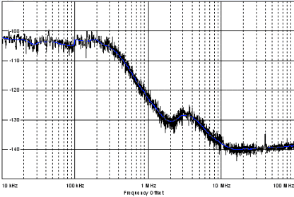
4.12 PLL Parameters
4.12.1 High Performance Mode
TA = 25°C, VDD = 3.0 V (unless otherwise noted)
| PARAMETER | MIN | TYP | MAX | UNIT | CONDITION |
|---|---|---|---|---|---|
| Phase noise in 868-, 915-, and 920-MHz Bands 200-kHz loop bandwidth setting |
–94 | dBc/Hz | ± 10 kHz offset | ||
| –96 | dBc/Hz | ± 100 kHz offset | |||
| –123 | dBc/Hz | ± 1 MHz offset | |||
| –137 | dBc/Hz | ± 10 MHz offset | |||
| Phase noise in 868-, 915-, and 920-MHz Bands 300-kHz loop bandwidth setting |
–100 | dBc/Hz | ± 10 kHz offset | ||
| –102 | dBc/Hz | ± 100 kHz offset | |||
| –121 | dBc/Hz | ± 1 MHz offset | |||
| –136 | dBc/Hz | ± 10 MHz offset | |||
| Phase noise in 868-, 915-, and 920-MHz Bands 400-kHz loop bandwidth setting |
–103 | dBc/Hz | ± 10 kHz offset | ||
| –104 | dBc/Hz | ± 100 kHz offset | |||
| –119 | dBc/Hz | ± 1 MHz offset | |||
| –133 | dBc/Hz | ± 10 MHz offset | |||
| Phase noise in 868-, 915-, and 920-MHz Bands 500-kHz loop bandwidth setting |
–104 | dBc/Hz | ± 10 kHz offset | ||
| –106 | dBc/Hz | ± 100 kHz offset | |||
| –116 | dBc/Hz | ± 1 MHz offset | |||
| –130 | dBc/Hz | ± 10 MHz offset | |||
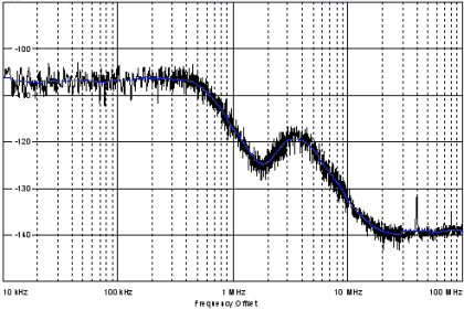
| Phase noise in 433-MHz band 300-kHz loop bandwidth setting |
–106 | dBc/Hz | ± 10 kHz offset | ||
| –107 | dBc/Hz | ± 100 kHz offset | |||
| –127 | dBc/Hz | ± 1 MHz offset | |||
| –141 | dBc/Hz | ± 10 MHz offset | |||
| Phase noise in 169-MHz band 300-kHz loop bandwidth setting |
–114 | dBc/Hz | ± 10 kHz offset | ||
| –114 | dBc/Hz | ± 100 kHz offset | |||
| –132 | dBc/Hz | ± 1 MHz offset | |||
| –142 | dBc/Hz | ± 10 MHz offset |
4.12.2 Low-Power Mode
| PARAMETER | MIN | TYP | MAX | UNIT | CONDITION | |
|---|---|---|---|---|---|---|
| Phase noise in 868-, 915-, and 920-MHz bands 200-kHz loop bandwidth setting |
–99 | dBc/Hz | ± 10 kHz offset | |||
| –101 | dBc/Hz | ± 100 kHz offset | ||||
| –121 | dBc/Hz | ± 1 MHz offset | ||||
| –135 | dBc/Hz | ± 10 MHz offset | ||||
4.13 Wake-up and Timing
TA = 25°C, VDD = 3.0 V, fc = 869.5 MHz (unless otherwise noted)
The turnaround behavior to and from RX and/or TX is highly configurable, and the time it takes will depend on how the device is set up. See the CC120X user guide (SWRU346) for more information.
| PARAMETER | MIN | TYP | MAX | UNIT | CONDITION |
|---|---|---|---|---|---|
| Powerdown to IDLE | 0.24 | ms | Depends on crystal | ||
| IDLE to RX/TX | 133 | µs | Calibration disabled | ||
| 369 | µs | Calibration enabled | |||
| RX/TX turnaround | 43 | µs | |||
| RX-to-RX turnaround | 369 | µs | With PLL calibration | ||
| 0 | µs | Without PLL calibration | |||
| TX-to-TX turnaround | 369 | µs | With PLL calibration | ||
| 0 | µs | Without PLL calibration | |||
| RX/TX to IDLE time | 237 | µs | Calibrate when leaving RX/TX enabled | ||
| 0 | µs | Calibrate when leaving RX/TX disabled | |||
| Frequency synthesizer calibration | 314 | µs | When using SCAL strobe | ||
| Minimum required number of preamble bytes | 0.5 | bytes | Required for RF front end gain settling only. Digital demodulation does not require preamble for settling | ||
| Time from start RX until valid RSSI(1)
Including gain settling (function of channel bandwidth. Programmable for trade-off between speed and accuracy) |
0.25 | ms | 120-kHz channels |
4.14 40-MHz Crystal Oscillator
TA = 25°C, VDD = 3.0 V (unless otherwise noted)
| PARAMETER | MIN | TYP | MAX | UNIT | CONDITION |
|---|---|---|---|---|---|
| Crystal frequency | 38.4 | 40 | MHz | It is expected that there will be degraded sensitivity at multiples of XOSC/2 in RX, and an increase in spurious emissions when the RF channel is close to multiples of XOSC in TX. We recommend that the RF channel is kept RX_BW/2 away from XOSC/2 in RX, and that the level of spurious emissions be evaluated if the RF channel is closer than 1 MHz to multiples of XOSC in TX. | |
| Load capacitance (CL) | 10 | pF | |||
| ESR | 60 | Ω | Simulated over operating conditions | ||
| Start-up time | 0.24 | ms | Depends on crystal |
4.15 40-MHz Clock Input (TCXO)
TA = 25°C, VDD = 3.0 V if nothing else stated
| PARAMETER | MIN | TYP | MAX | UNIT | CONDITION |
|---|---|---|---|---|---|
| Clock frequency | 38.4 | 40 | MHz | ||
| TCXO with CMOS output | TCXO with CMOS output directly coupled to pin EXT_OSC | ||||
| High input voltage | 1.4 | VDD | V | ||
| Low input voltage | 0 | 0.6 | V | ||
| Rise / Fall time | 2 | ns | |||
| Clipped sine output | TCXO clipped sine output connected to pin EXT_OSC through series capacitor | ||||
| Clock input amplitude (peak-to-peak) | 0.8 | 1.5 | V |
4.16 32-kHz Clock Input
TA = 25°C, VDD = 3.0 V (unless otherwise noted)
| PARAMETER | MIN | TYP | MAX | UNIT | CONDITION |
|---|---|---|---|---|---|
| Clock frequency | 32 | kHz | |||
| 32-kHz clock input pin input high voltage | 0.8 x VDD | V | |||
| 32-kHz clock input pin input low voltage | 0.2 x VDD | V |
4.17 40-kHz RC Oscillator
TA = 25°C, VDD = 3.0 V (unless otherwise noted)
| PARAMETER | MIN | TYP | MAX | UNIT | CONDITION |
|---|---|---|---|---|---|
| Frequency | 40 | kHz | After calibration (frequency calibrated against the 40-MHz crystal or TCXO) | ||
| Frequency accuracy after calibration | ±0.1 | % | Relative to frequency reference (that is, 40-MHz crystal or TCXO) | ||
| Initial calibration time | 1.32 | ms |
4.18 I/O and Reset
TA = 25°C, VDD = 3.0 V (unless otherwise noted)
| PARAMETER | MIN | TYP | MAX | UNIT | CONDITION |
|---|---|---|---|---|---|
| Logic input high voltage | 0.8 x VDD | V | |||
| Logic input low voltage | 0.2 x VDD | V | |||
| Logic output high voltage | 0.8 x VDD | V | At 4-mA output load or less | ||
| Logic output low voltage | 0.2 x VDD | V | |||
| Power-on reset threshold | 1.3 | V | Voltage on DVDD pin |
4.19 Temperature Sensor
TA = 25°C, VDD = 3.0 V (unless otherwise noted).
| PARAMETER | MIN | TYP | MAX | UNIT | CONDITION |
|---|---|---|---|---|---|
| Temperature sensor range | –40 | 85 | °C | ||
| Temperature coefficient | 2.66 | mV / °C | Change in sensor output voltage versus change in temperature | ||
| Typical output voltage | 794 | mV | Typical sensor output voltage at TA = 25°C, VDD = 3.0 V | ||
| VDD coefficient | 1.17 | mV / V | Change in sensor output voltage versus change in VDD |
The CC1201 device can be configured to provide a voltage proportional to temperature on GPIO1. The temperature can be estimated by measuring this voltage (see Section 4.19, Temperature Sensor). For more information, see the temperature sensor design note (SWRA415).
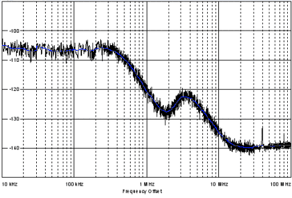
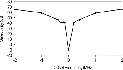
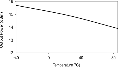
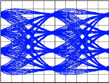
4.20 Typical Characteristics
TA = 25°C, VDD = 3.0 V, fc = 869.5 MHz (unless otherwise noted)
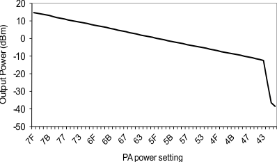
vs PA Power Setting
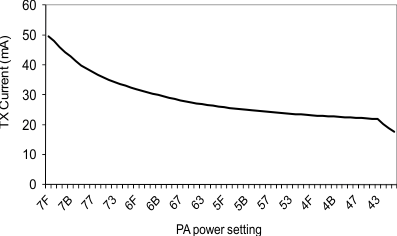
vs PA Power Setting
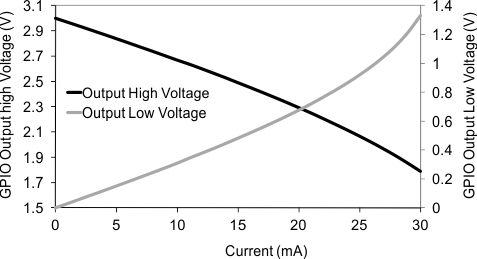
vs Current Being Sourced and Sinked