SWRS037B January 2006 – March 2015 CC1150
PRODUCTION DATA.
- 1Device Overview
- 2Revision History
- 3Terminal Configuration and Functions
-
4Specifications
- 4.1 Absolute Maximum Ratings
- 4.2 ESD Ratings
- 4.3 Recommended Operating Conditions
- 4.4 General Characteristics
- 4.5 Current Consumption
- 4.6 RF Transmit
- 4.7 Crystal Oscillator
- 4.8 Frequency Synthesizer Characteristics
- 4.9 Analog Temperature Sensor
- 4.10 DC Characteristics
- 4.11 Power-On Reset
- 4.12 Thermal Resistance Characteristics for VQFNP Package
-
5Detailed Description
- 5.1 Overview
- 5.2 Functional Block Diagram
- 5.3 Configuration Overview
- 5.4 Configuration Software
- 5.5 4-wire Serial Configuration and Data Interface
- 5.6 Microcontroller Interface and Pin Configuration
- 5.7 Data Rate Programming
- 5.8 Packet Handling Hardware Support
- 5.9 Modulation Formats
- 5.10 Forward Error Correction with Interleaving
- 5.11 Radio Control
- 5.12 Data FIFO
- 5.13 Frequency Programming
- 5.14 VCO
- 5.15 Voltage Regulators
- 5.16 Output Power Programming
- 5.17 General Purpose and Test Output Control Pins
- 5.18 Asynchronous and Synchronous Serial Operation
- 5.19 System Considerations and Guidelines
- 5.20 Memory
- 6Applications, Implementation, and Layout
- 7Device and Documentation Support
- 8Mechanical Packaging and Orderable Information
3 Terminal Configuration and Functions
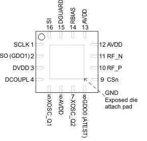
The CC1150 pinout is shown in Figure 3-1 and Table 3-1
 Figure 3-1 Pinout Top View
3.1 Pin Attributes
Table 3-1 Pin Attributes(1)
| PIN NO. | PIN NAME | TYPE | DESCRIPTION |
|---|---|---|---|
| 1 | SCLK | Digital Input | Serial configuration interface, clock input. |
| 2 | SO (GDO1) | Digital Output | Serial configuration interface, data output. Optional general output pin when CSn is high. |
| 3 | DVDD | Power (Digital) | 1.8-V to 3.6-V digital power supply for digital I/Os and for the digital core voltage regulator. |
| 4 | DCOUPL(2) | Power (Digital) | 1.6-V to 2.0-V digital power supply output for decoupling. |
| 5 | XOSC_Q1 | Analog I/O | Crystal oscillator pin 1, or external clock input. |
| 6 | AVDD | Power (Analog) | 1.8-V to 3.6-V analog power supply connection. |
| 7 | XOSC_Q2 | Analog I/O | Crystal oscillator pin 2. |
| 8 | GDO0 (ATEST) |
Digital I/O | Digital output pin for general use:
|
| 9 | CSn | Digital Input | Serial configuration interface, chip select. |
| 10 | RF_P | RF I/O | Positive RF output signal from PA. |
| 11 | RF_N | RF I/O | Negative RF output signal from PA. |
| 12 | AVDD | Power (Analog) | 1.8-V to 3.6-V analog power supply connection. |
| 13 | AVDD | Power (Analog) | 1.8-V to 3.6-V analog power supply connection. |
| 14 | RBIAS | Analog I/O | External bias resistor for reference current. |
| 15 | DGUARD | Power (Digital) | Power supply connection for digital noise isolation. |
| 16 | SI | Digital Input | Serial configuration interface, data input. |
(1) The exposed die attach pad must be connected to a solid ground plane as this is the main ground connection for the chip.
(2) This pin is intended for use with the CC1150 only. It can not be used to provide supply voltage to other devices.