ZHCSE72 September 2015
PRODUCTION DATA.
- 1 特性
- 2 应用
- 3 说明
- 4 简化电路原理图
- 5 修订历史记录
- 6 Pin Configuration and Functions
-
7 Specifications
- 7.1 Absolute Maximum Ratings
- 7.2 ESD Ratings
- 7.3 Recommended Operating Conditions
- 7.4 Supply Current
- 7.5 Power Supply Control
- 7.6 Low-Voltage General Purpose I/O, TS1
- 7.7 Power-On Reset (POR)
- 7.8 Internal 1.8-V LDO
- 7.9 Current Wake Comparator
- 7.10 Coulomb Counter
- 7.11 ADC Digital Filter
- 7.12 ADC Multiplexer
- 7.13 Cell Balancing Support
- 7.14 Internal Temperature Sensor
- 7.15 NTC Thermistor Measurement Support
- 7.16 High-Frequency Oscillator
- 7.17 Low-Frequency Oscillator
- 7.18 Voltage Reference 1
- 7.19 Voltage Reference 2
- 7.20 Instruction Flash
- 7.21 Data Flash
- 7.22 Current Protection Thresholds
- 7.23 Current Protection Timing
- 7.24 N-CH FET Drive (CHG, DSG)
- 7.25 I2C and HDQ Interface I/O
- 7.26 I2C Interface Timing
- 7.27 HDQ Interface Timing
- 7.28 Typical Characteristics
-
8 Detailed Description
- 8.1 Overview
- 8.2 Functional Block Diagram
- 8.3
Feature Description
- 8.3.1 Battery Parameter Measurements
- 8.3.2 Coulomb Counter (CC)
- 8.3.3 CC Digital Filter
- 8.3.4 ADC Multiplexer
- 8.3.5 Analog-to-Digital Converter (ADC)
- 8.3.6 ADC Digital Filter
- 8.3.7 Internal Temperature Sensor
- 8.3.8 External Temperature Sensor Support
- 8.3.9 Power Supply Control
- 8.3.10 Power-On Reset
- 8.3.11 Bus Communication Interface
- 8.3.12 Cell Balancing Support
- 8.3.13 N-Channel Protection FET Drive
- 8.3.14 Low Frequency Oscillator
- 8.3.15 High Frequency Oscillator
- 8.3.16 1.8-V Low Dropout Regulator
- 8.3.17 Internal Voltage References
- 8.3.18 Overcurrent in Discharge Protection
- 8.3.19 Short-Circuit Current in Charge Protection
- 8.3.20 Short-Circuit Current in Discharge 1 and 2 Protection
- 8.3.21 Primary Protection Features
- 8.3.22 Gas Gauging
- 8.3.23 Charge Control Features
- 8.3.24 Authentication
- 8.4 Device Functional Modes
- 9 Applications and Implementation
- 10Power Supply Requirements
- 11Layout
- 12器件和文档支持
- 13机械、封装和可订购信息
7 Specifications
7.1 Absolute Maximum Ratings
Over operating free-air temperature range (unless otherwise noted)(1)| MIN | MAX | UNIT | ||
|---|---|---|---|---|
| Supply voltage range, VCC | VC2, PBI | –0.3 | 30 | V |
| Input voltage range, VIN | PACK | –0.3 | 30 | V |
| TS1 | –0.3 | VREG + 0.3 | V | |
| SRP, SRN | –0.3 | 0.3 | V | |
| VC2 | VC1 – 0.3 | VC1 + 8.5 or VSS + 30 | V | |
| VC1 | VSS – 0.3 | VSS + 8.5 or VSS + 30 | V | |
| Output voltage range, VO | CHG, DSG | –0.3 | 32 | V |
| Maximum VSS current, ISS | ±50 | mA | ||
| Functional Temperature, TFUNC | –40 | 110 | °C | |
| Lead temperature (soldering, 10 s), TSOLDER | ±300 | |||
| Storage temperature range, TSTG | –65 | 150 | °C | |
(1) Stresses beyond those listed under absolute maximum ratings may cause permanent damage to the device. These are stress ratings only, and functional operation of the device at these or any other conditions beyond those indicated under recommended operating conditions is not implied. Exposure to absolute–maximum–rated conditions for extended periods may affect device reliability.
7.2 ESD Ratings
| VALUE | UNIT | |||
|---|---|---|---|---|
| V(ESD) | Electrostatic discharge | Human body model (HBM), per ANSI/ESDA/JEDEC JS-001, all pins(1) | ±2000 | V |
| Charged device model (CDM), per JEDEC specification JESD22-C101, all pins(2) | ±500 | |||
(1) JEDEC document JEP155 states that 500-V HBM allows safe manufacturing with a standard ESD control process.
(2) JEDEC document JEP157 states that 250-V CDM allows safe manufacturing with a standard ESD control process.
7.3 Recommended Operating Conditions
Typical values stated where TA = 25ºC and VCC = 7.2 V, Min/Max values stated where TA = –40ºC to 85ºC and VCC = 2.2 V to 26 V (unless otherwise noted)| MIN | NOM | MAX | UNIT | ||||
|---|---|---|---|---|---|---|---|
| VCC | Supply voltage | VC2, PBI | 2.2 | 26 | V | ||
| VSHUTDOWN– | Shutdown voltage | VPACK < VSHUTDOWN– | 1.8 | 2.0 | 2.2 | V | |
| VSHUTDOWN+ | Start-up voltage | VPACK > VSHUTDOWN– + VHYS | 2.05 | 2.25 | 2.45 | V | |
| VHYS | Shutdown voltage hysteresis | VSHUTDOWN+ – VSHUTDOWN– | 250 | mV | |||
| VIN | Input voltage range | SDA/HDQ, SCL | 5.5 | V | |||
| TS1 | VREG | ||||||
| SRP, SRN | –0.2 | 0.2 | |||||
| VC2 | VVC1 | VVC1 + 5 | |||||
| VC1 | VVSS | VVSS + 5 | |||||
| PACK | 26 | ||||||
| VO | Output voltage range | CHG, DSG | 26 | V | |||
| CPBI | External PBI capacitor | 2.2 | µF | ||||
| TOPR | Operating temperature | –40 | 85 | °C | |||
Thermal Information
over operating free-air temperature range (unless otherwise noted)| THERMAL METRIC(1) | bq78z100 | UNIT | |
|---|---|---|---|
| DRZ | |||
| 12 PINS | |||
| RθJA, High K | Junction-to-ambient thermal resistance | 186.4 | °C/W |
| RθJC(top) | Junction-to-case(top) thermal resistance | 90.4 | |
| RθJB | Junction-to-board thermal resistance | 110.7 | |
| ψJT | Junction-to-top characterization parameter | 96.7 | |
| ψJB | Junction-to-board characterization parameter | 90 | |
| RθJC(bottom) | Junction-to-case(bottom) thermal resistance | n/a | |
(1) For more information about traditional and new thermal metrics, see the Semiconductor and IC Package Thermal Metrics application report, SPRA953.
7.4 Supply Current
Typical values stated where TA = 25ºC and VCC = 7.2 V, Min/Max values stated where TA = –40ºC to 85ºC and VCC = 2.2 V to 7.6 V (unless otherwise noted)| PARAMETER | TEST CONDITION | MIN | TYP | MAX | UNIT | ||
|---|---|---|---|---|---|---|---|
| INORMAL | NORMAL mode | CHG = ON, DSG = ON, No Flash Write and CPU = ON | 400 | 500 | µA | ||
| CHG = ON, DSG = ON, No Flash Write and CPU = Halted | 250 | 300 | |||||
| ISLEEP | SLEEP mode | CHG = OFF, DSG = ON, No Communication on Bus | 90 | 160 | µA | ||
| CHG = OFF, DSG = OFF, No Communication on Bus | 38 | 120 | |||||
| ISHUTDOWN | SHUTDOWN mode | 0.5 | 2 | µA | |||
7.5 Power Supply Control
Typical values stated where TA = 25ºC and VCC = 7.2 V, Min/Max values stated where TA = –40ºC to 85ºC and VCC = 2.2 V to 7.6 V (unless otherwise noted)| PARAMETER | TEST CONDITION | MIN | TYP | MAX | UNIT | |
|---|---|---|---|---|---|---|
| VSWITCHOVER– | VC2 to PACK switchover voltage | VVC2 < VSWITCHOVER– | 2.0 | 2.1 | 2.2 | V |
| VSWITCHOVER+ | PACK to VC2 switchover voltage | VVC2 > VSWITCHOVER– + VHYS | 3.0 | 3.1 | 3.2 | V |
| VHYS | Switchover voltage hysteresis | VSWITCHOVER+ – VSWITCHOVER– | 1000 | mV | ||
| ILKG | Input Leakage current | VC2 pin, VC2 = 0 V, PACK = 25 V | 1 | µA | ||
| PACK pin, VC2 = 25 V, PACK = 0 V | 1 | |||||
| VC2 and PACK pins, VC2 = 0 V, PACK = 0 V, PBI = 25 V | 1 | |||||
| RPACK(PD) | Internal pulldown resistance | PACK | 30 | 40 | 50 | kΩ |
7.6 Low-Voltage General Purpose I/O, TS1
Typical values stated where TA = 25ºC and VCC = 7.2 V, Min/Max values stated where TA = –40ºC to 85ºC and VCC = 2.2 V to 7.6 V (unless otherwise noted)| PARAMETER | TEST CONDITION | MIN | TYP | MAX | UNIT | |
|---|---|---|---|---|---|---|
| VIH | High-level input | 0.65 x VREG | V | |||
| VIL | Low-level input | 0.35 x VREG | V | |||
| VOH | Output voltage high | IOH = – 1.0 mA | 0.75 x VREG | V | ||
| VOL | Output voltage low | IOL = 1.0 mA | 0.2 x VREG | V | ||
| CIN | Input capacitance | 5 | pF | |||
| ILKG | Input leakage current | 1 | µA | |||
7.7 Power-On Reset (POR)
Typical values stated where TA = 25ºC and VCC = 7.2 V, Min/Max values stated where TA = –40ºC to 85ºC and VCC = 2.2 V to 7.6 V (unless otherwise noted)| PARAMETER | TEST CONDITION | MIN | TYP | MAX | UNIT | |
|---|---|---|---|---|---|---|
| VREGIT– | Negative-going voltage input | VREG | 1.51 | 1.55 | 1.59 | V |
| VHYS | Power-on reset hysteresis | VREGIT+ – VREGIT– | 70 | 100 | 130 | mV |
| tRST | Power-on reset time | 200 | 300 | 400 | µs | |
7.8 Internal 1.8-V LDO
Typical values stated where TA = 25ºC and VCC = 7.2 V, Min/Max values stated where TA = –40ºC to 85ºC and VCC = 2.2 V to 7.6 V (unless otherwise noted)| PARAMETER | TEST CONDITION | MIN | TYP | MAX | UNIT | ||
|---|---|---|---|---|---|---|---|
| VREG | Regulator voltage | 1.6 | 1.8 | 2.0 | V | ||
| ΔVO(TEMP) | Regulator output over temperature | ΔVREG/ΔTA, IREG = 10 mA | ±0.25% | ||||
| ΔVO(LINE) | Line regulation | ΔVREG/ΔVBAT, VBAT = 10 mA | –0 .6% | 0.5% | |||
| ΔVO(LOAD) | Load regulation | ΔVREG/ΔIREG, IREG = 0 mA to 10 mA | –1.5% | 1.5% | |||
| IREG | Regulator output current limit | VREG = 0.9 x VREG(NOM), VIN > 2.2 V | 20 | mA | |||
| ISC | Regulator short-circuit current limit | VREG = 0 x VREG(NOM) | 25 | 40 | 50 | mA | |
| PSRRREG | Power supply rejection ratio | ΔVBAT/ΔVREG, IREG = 10 mA, VIN > 2.5 V, f = 10 Hz | 40 | dB | |||
| VSLEW | Slew rate enhancement voltage threshold | VREG | 1.58 | 1.65 | V | ||
7.9 Current Wake Comparator
Typical values stated where TA = 25ºC and VCC = 7.2 V, Min/Max values stated where TA = –40ºC to 85ºC and VCC = 2.2 V to 7.6 V (unless otherwise noted)| PARAMETER | TEST CONDITION | MIN | TYP | MAX | UNIT | |
|---|---|---|---|---|---|---|
| VWAKE | Wake voltage threshold | VWAKE = VSRP – VSRN WAKE_CONTROL[WK1, WK0] = 0,0 | ±0.3 | ±0.625 | ±0.9 | mV |
| VWAKE = VSRP – VSRN WAKE_CONTROL[WK1, WK0] = 0,1 | ±0.6 | ±1.25 | ±1.8 | mV | ||
| VWAKE = VSRP – VSRN WAKE_CONTROL[WK1, WK0] = 1,0 | ±1.2 | ±2.5 | ±3.6 | mV | ||
| VWAKE = VSRP – VSRN WAKE_CONTROL[WK1, WK0] = 1,1 | ±2.4 | ±5.0 | ±7.2 | mV | ||
| VWAKE(DRIFT) | Temperature drift of VWAKE accuracy | 0.5% | °C | |||
| tWAKE | Time from application of current to wake | 0.25 | 0.5 | ms | ||
| tWAKE(SU) | Wake up comparator startup time | [WKCHGEN] = 0 and [WKDSGEN] = 0 to [WKCHGEN] = 1 and [WKDSGEN] = 1 | 250 | 640 | µs | |
7.10 Coulomb Counter
Typical values stated where TA = 25ºC and VCC = 7.2 V, Min/Max values stated where TA = –40ºC to 85ºC and VCC = 2.2 V to 7.6 V (unless otherwise noted)| PARAMETER | TEST CONDITION | MIN | TYP | MAX | UNIT |
|---|---|---|---|---|---|
| Input voltage range | –100 | 100 | mV | ||
| Full scale range | –VREF1/10 | +VREF1/10 | mV | ||
| Differential nonlinearity | 16-bit, No missing codes | ±1 | LSB | ||
| Integral nonlinearity | 16-bit, Best fit over input voltage range | ±5.2 | ±22.3 | LSB | |
| Offset error | 16-bit, Post-calibration | ±1.3 | ±2.6 | LSB | |
| Offset error drift | 15-bit + sign, Post-calibration | 0.04 | 0.07 | LSB/°C | |
| Gain error | 15-bit + sign, Over input voltage range | ±131 | ±492 | LSB | |
| Gain error drift | 15-bit + sign, Over input voltage range | 4.3 | 9.8 | LSB/°C | |
| Effective input resistance | 2.5 | MΩ |
7.11 ADC Digital Filter
Typical values stated where TA = 25ºC and VCC = 7.2 V, Min/Max values stated where TA = –40ºC to 85ºC and VCC = 2.2 V to 7.6 V (unless otherwise noted)| PARAMETER | TEST CONDITION | MIN | TYP | MAX | UNIT |
|---|---|---|---|---|---|
| tCONV | ADCTL[SPEED1, SPEED0] = 0, 0 | 31.25 | ms | ||
| ADCTL[SPEED1, SPEED0] = 0, 1 | 15.63 | ||||
| ADCTL[SPEED1, SPEED0] = 1, 0 | 7.81 | ||||
| ADCTL[SPEED1, SPEED0] = 1, 1 | 1.95 | ||||
| Resolution | No missing codes, ADCTL[SPEED1, SPEED0] = 0, 0 | 16 | Bits | ||
| Effective resolution | With sign, ADCTL[SPEED1, SPEED0] = 0, 0 | 14 | 15 | Bits | |
| With sign, ADCTL[SPEED1, SPEED0] = 0, 1 | 13 | 14 | |||
| With sign, ADCTL[SPEED1, SPEED0] = 1, 0 | 11 | 12 | |||
| With sign, ADCTL[SPEED1, SPEED0] = 1, 1 | 9 | 10 |
7.12 ADC Multiplexer
Typical values stated where TA = 25ºC and VCC = 7.2 V, Min/Max values stated where TA = –40ºC to 85ºC and VCC = 2.2 V to 7.6 V (unless otherwise noted)| PARAMETER | TEST CONDITION | MIN | TYP | MAX | UNIT | |
|---|---|---|---|---|---|---|
| K | Scaling factor | VC1–VSS, VC2–VC1 | 0.1980 | 0.2000 | 0.2020 | — |
| VC2–VSS, PACK–VSS | 0.0485 | 0.050 | 0.051 | |||
| VREF1/2 | 0.490 | 0.500 | 0.510 | |||
| VIN | Input voltage range | VC2–VSS, PACK–VSS | –0.2 | 20 | V | |
| TS1 | –0.2 | 0.8 × VREF1 | ||||
| TS1 | –0.2 | 0.8 × VREG | ||||
| ILKG | Input leakage current | VC1, VC2 cell balancing off, cell detach detection off, ADC multiplexer off | 1 | µA | ||
7.13 Cell Balancing Support
Typical values stated where TA = 25ºC and VCC = 7.2 V, Min/Max values stated where TA = –40ºC to 85ºC and VCC = 2.2 V to 7.6 V (unless otherwise noted)| PARAMETER | TEST CONDITION | MIN | TYP | MAX | UNIT | |
|---|---|---|---|---|---|---|
| RCB | Internal cell balance resistance | RDS(ON) for internal FET switch at 2 V < VDS < 4 V | 200 | Ω | ||
7.14 Internal Temperature Sensor
Typical values stated where TA = 25ºC and VCC = 7.2 V, Min/Max values stated where TA = –40ºC to 85ºC and VCC = 2.2 V to 7.6 V (unless otherwise noted)| PARAMETER | TEST CONDITION | MIN | TYP | MAX | UNIT | |
|---|---|---|---|---|---|---|
| VTEMP | Internal temperature sensor voltage drift | VTEMPP | –1.9 | –2.0 | –2.1 | mV/°C |
| VTEMPP – VTEMPN (1) | 0.177 | 0.178 | 0.179 | |||
(1) Assured by design
7.15 NTC Thermistor Measurement Support
Typical values stated where TA = 25ºC and VCC = 7.2 V, Min/Max values stated where TA = –40ºC to 85ºC and VCC = 2.2 V to 7.6 V (unless otherwise noted)| PARAMETER | TEST CONDITION | MIN | TYP | MAX | UNIT | |
|---|---|---|---|---|---|---|
| RNTC(PU) | Internal pull-up resistance | TS1 | 14.4 | 18 | 21.6 | kΩ |
| RNTC(DRIFT) | Resistance drift over temperature | TS1 | –360 | –280 | –200 | PPM/°C |
7.16 High-Frequency Oscillator
Typical values stated where TA = 25ºC and VCC = 7.2 V, Min/Max values stated where TA = –40ºC to 85ºC and VCC = 2.2 V to 7.6 V (unless otherwise noted)| PARAMETER | TEST CONDITION | MIN | TYP | MAX | UNIT | |
|---|---|---|---|---|---|---|
| fHFO | Operating frequency | 16.78 | MHz | |||
| fHFO(ERR) | Frequency error | TA = –20°C to 70°C, includes frequency drift | –2.5% | ±0.25% | 2.5% | |
| TA = –40°C to 85°C, includes frequency drift | –3.5% | ±0.25% | 3.5% | |||
| tHFO(SU) | Start-up time | TA = –20°C to 85°C, Oscillator frequency within +/–3% of nominal, CLKCTL[HFRAMP] = 1 | 4 | ms | ||
| Oscillator frequency within +/–3% of nominal, CLKCTL[HFRAMP] = 0 | 100 | µs | ||||
7.17 Low-Frequency Oscillator
Typical values stated where TA = 25ºC and VCC = 7.2 V, Min/Max values stated where TA = –40ºC to 85ºC and VCC = 2.2 V to 7.6 V (unless otherwise noted)| PARAMETER | TEST CONDITION | MIN | TYP | MAX | UNIT | |
|---|---|---|---|---|---|---|
| fLFO | Operating frequency | 262.144 | kHz | |||
| fLFO(LP) | Operating frequency in low power mode | 247 | kHz | |||
| fLFO(ERR) | Frequency error | TA = –20°C to 70°C, includes frequency drift | –1.5% | ±0.25% | 1.5% | |
| TA = –40°C to 85°C, includes frequency drift | –2.5% | ±0.25% | 2.5% | |||
| fLFO(LPERR) | Frequency error in low power mode | –5% | 5% | |||
| fLFO(FAIL) | Failure detection frequency | 30 | 80 | 100 | kHz | |
7.18 Voltage Reference 1
Typical values stated where TA = 25ºC and VCC = 7.2 V, Min/Max values stated where TA = –40ºC to 85ºC and VCC = 2.2 V to 7.6 V (unless otherwise noted)| PARAMETER | TEST CONDITION | MIN | TYP | MAX | UNIT | |
|---|---|---|---|---|---|---|
| VREF1 | Internal reference voltage | TA = 25°C, after trim | 1.215 | 1.220 | 1.225 | V |
| VREF1(DRIFT) | Internal reference voltage drift | TA = 0°C to 60°C, after trim | ±50 | PPM/°C | ||
| TA = –40°C to 85°C, after trim | ±80 | |||||
7.19 Voltage Reference 2
Typical values stated where TA = 25ºC and VCC = 7.2 V, Min/Max values stated where TA = –40ºC to 85ºC and VCC = 2.2 V to 7.6 V (unless otherwise noted)| PARAMETER | TEST CONDITION | MIN | TYP | MAX | UNIT | |
|---|---|---|---|---|---|---|
| VREF2 | Internal reference voltage | TA = 25°C, after trim | 1.215 | 1.220 | 1.225 | V |
| VREF2(DRIFT) | Internal reference voltage drift | TA = 0°C to 60°C, after trim | ±50 | PPM/°C | ||
| TA = –40°C to 85°C, after trim | ±80 | |||||
7.20 Instruction Flash
Typical values stated where TA = 25ºC and VCC = 7.2 V, Min/Max values stated where TA = –40ºC to 85ºC and VCC = 2.2 V to 7.6 V (unless otherwise noted)| PARAMETER | TEST CONDITION | MIN | TYP | MAX | UNIT | |
|---|---|---|---|---|---|---|
| Data retention | 10 | Years | ||||
| Flash programming write cycles | 1000 | Cycles | ||||
| tPROGWORD | Word programming time | TA = –40°C to 85°C | 40 | µs | ||
| tMASSERASE | Mass-erase time | TA = –40°C to 85°C | 40 | ms | ||
| tPAGEERASE | Page-erase time | TA = –40°C to 85°C | 40 | ms | ||
| IFLASHREAD | Flash-read current | TA = –40°C to 85°C | 2 | mA | ||
| IFLASHWRITE | Flash-write current | TA = –40°C to 85°C | 5 | mA | ||
| IFLASHERASE | Flash-erase current | TA = –40°C to 85°C | 15 | mA | ||
7.21 Data Flash
Typical values stated where TA = 25ºC and VCC = 7.2 V, Min/Max values stated where TA = –40ºC to 85ºC and VCC = 2.2 V to 7.6 V (unless otherwise noted)| PARAMETER | TEST CONDITION | MIN | TYP | MAX | UNIT | |
|---|---|---|---|---|---|---|
| Data retention | 10 | Years | ||||
| Flash programming write cycles | 20000 | Cycles | ||||
| tPROGWORD | Word programming time | TA = –40°C to 85°C | 40 | µs | ||
| tMASSERASE | Mass-erase time | TA = –40°C to 85°C | 40 | ms | ||
| tPAGEERASE | Page-erase time | TA = –40°C to 85°C | 40 | ms | ||
| IFLASHREAD | Flash-read current | TA = –40°C to 85°C | 1 | mA | ||
| IFLASHWRITE | Flash-write current | TA = –40°C to 85°C | 5 | mA | ||
| IFLASHERASE | Flash-erase current | TA = –40°C to 85°C | 15 | mA | ||
7.22 Current Protection Thresholds
Typical values stated where TA = 25ºC and VCC = 7.2 V, Min/Max values stated where TA = –40ºC to 85ºC and VCC = 2.2 V to 7.6 V (unless otherwise noted)| PARAMETER | TEST CONDITION | MIN | TYP | MAX | UNIT | ||
|---|---|---|---|---|---|---|---|
| VOCD | OCD detection threshold voltage range | VOCD = VSRP – VSRN, PROTECTION_CONTROL[RSNS] = 1 | –16.6 | –100 | mV | ||
| VOCD = VSRP – VSRN, PROTECTION_CONTROL[RSNS] = 0 | –8.3 | –50 | |||||
| ΔVOCD | OCD detection threshold voltage program step | VOCD = VSRP – VSRN, PROTECTION_CONTROL[RSNS] = 1 | –5.56 | mV | |||
| VOCD = VSRP – VSRN, PROTECTION_CONTROL[RSNS] = 0 | –2.78 | ||||||
| ΔVSCC | SCC detection threshold voltage range | VSCC = VSRP – VSRN, PROTECTION_CONTROL[RSNS] = 1 | 44.4 | 200 | mV | ||
| VSCC = VSRP – VSRN, PROTECTION_CONTROL[RSNS] = 0 | 22.2 | 100 | |||||
| ΔVSCC | SCC detection threshold voltage program step | VSCC = VSRP – VSRN, PROTECTION_CONTROL[RSNS] = 1 | 22.2 | mV | |||
| VSCC = VSRP – VSRN, PROTECTION_CONTROL[RSNS] = 0 | 11.1 | ||||||
| VSCD1 | SCD1 detection threshold voltage range | VSCD1 = VSRP – VSRN, PROTECTION_CONTROL[RSNS] = 1 | –44.4 | –200 | mV | ||
| VSCD1 = VSRP – VSRN, PROTECTION_CONTROL[RSNS] = 0 | –22.2 | –100 | |||||
| ΔVSCD1 | SCD1 detection threshold voltage program step | VSCD1 = VSRP – VSRN, PROTECTION_CONTROL[RSNS] = 1 | –22.2 | mV | |||
| VSCD1 = VSRP – VSRN, PROTECTION_CONTROL[RSNS] = 0 | –11.1 | ||||||
| VSCD2 | SCD2 detection threshold voltage range | VSCD2 = VSRP – VSRN, PROTECTION_CONTROL[RSNS] = 1 | –44.4 | –200 | mV | ||
| VSCD2 = VSRP – VSRN, PROTECTION_CONTROL[RSNS] = 0 | –22.2 | –100 | |||||
| ΔVSCD2 | SCD2 detection threshold voltage program step | VSCD2 = VSRP – VSRN, PROTECTION_CONTROL[RSNS] = 1 | –22.2 | mV | |||
| VSCD2 = VSRP – VSRN, PROTECTION_CONTROL[RSNS] = 0 | –11.1 | ||||||
7.23 Current Protection Timing
Typical values stated where TA = 25ºC and VCC = 7.2 V, Min/Max values stated where TA = –40ºC to 85ºC and VCC = 2.2 V to 7.6 V (unless otherwise noted)| PARAMETER | TEST CONDITION | MIN | TYP | MAX | UNIT | |
|---|---|---|---|---|---|---|
| tOCD | OCD detection delay time | 1 | 31 | ms | ||
| ΔtOCD | OCD detection delay time program step | 2 | ms | |||
| tSCC | SCC detection delay time | 0 | 915 | µs | ||
| ΔtSCC | SCC detection delay time program step | 61 | µs | |||
| tSCD1 | SCD1 detection delay time | PROTECTION_CONTROL[SCDDx2] = 0 | 0 | 915 | µs | |
| PROTECTION_CONTROL[SCDDx2] = 1 | 0 | 1850 | ||||
| ΔtSCD1 | SCD1 detection delay time program step | PROTECTION_CONTROL[SCDDx2] = 0 | 61 | µs | ||
| PROTECTION_CONTROL[SCDDx2] = 1 | 121 | |||||
| tSCD2 | SCD2 detection delay time | PROTECTION_CONTROL[SCDDx2] = 0 | 0 | 458 | µs | |
| PROTECTION_CONTROL[SCDDx2] = 1 | 0 | 915 | ||||
| ΔtSCD2 | SCD2 detection delay time program step | PROTECTION_CONTROL[SCDDx2] = 0 | 30.5 | µs | ||
| PROTECTION_CONTROL[SCDDx2] = 1 | 61 | |||||
| tDETECT | Current fault detect time | VSRP – VSRN = VT – 3 mV for OCD, SCD1, and SC2, VSRP – VSRN = VT + 3 mV for SCC | 160 | µs | ||
| tACC | Current fault delay time accuracy | Max delay setting | –10% | 10% | ||
7.24 N-CH FET Drive (CHG, DSG)
Typical values stated where TA = 25ºC and VCC = 7.2 V, Min/Max values stated where TA = –40ºC to 85ºC and VCC = 2.2 V to 7.6 V (unless otherwise noted)| PARAMETER | TEST CONDITION | MIN | TYP | MAX | UNIT | ||
|---|---|---|---|---|---|---|---|
| Output voltage ratio | RatioDSG = (VDSG – VVC2)/VVC2, 2.2 V < VVC2 < 4.07 V, 10 MΩ between PACK and DSG | 2.133 | 2.333 | 2.467 | — | ||
| RatioCHG = (VCHG – VVC2)/VVC2, 2.2 V < VVC2 < 4.07 V, 10 MΩ between BAT and CHG | 2.133 | 2.333 | 2.467 | ||||
| V(FETON) | Output voltage, CHG and DSG on | VDSG(ON) = VDSG – VVC2, VVC2 ≥ 4.07 V, 10 MΩ between PACK and DSG, VVC2 = 18 V | 8.75 | 9.5 | 10.25 | V | |
| VCHG(ON) = VCHG – VVC2, VVC2 ≥ 4.07 V, 10 MΩ between VC2 and CHG, VVC2 = 18 V | 8.75 | 9.5 | 10.25 | ||||
| V(FETOFF) | Output voltage, CHG and DSG off | VDSG(OFF) = VDSG – VPACK, 10 MΩ between PACK and DSG | –0.4 | 0.4 | V | ||
| VCHG(OFF) = VCHG – VBAT, 10 MΩ between VC2 and CHG | –0.4 | 0.4 | |||||
| tR | Rise time | VDSG from 0% to 35% VDSG(ON)(TYP), VBAT ≥ 2.2 V, CL = 4.7 nF between DSG and PACK, 5.1 kΩ between DSG and CL, 10 MΩ between PACK and DSG | 200 | 500 | µs | ||
| VCHG from 0% to 35% VCHG(ON)(TYP), VVC2 ≥ 2.2 V, CL = 4.7 nF between CHG and VC2, 5.1 kΩ between CHG and CL, 10 MΩ between VC2 and CHG | 200 | 500 | |||||
| tF | Fall time | VDSG from VDSG(ON)(TYP) to 1 V, VVC2 ≥ 2.2 V, CL = 4.7 nF between DSG and PACK, 5.1 kΩ between DSG and CL, 10 MΩ between PACK and DSG | 40 | 300 | µs | ||
| VCHG from VCHG(ON)(TYP) to 1 V, VVC2 ≥ 2.2 V, CL = 4.7 nF between CHG and VC2, 5.1 kΩ between CHG and CL, 10 MΩ between VC2 and CHG | 40 | 200 | |||||
7.25 I2C and HDQ Interface I/O
Typical values stated where TA = 25ºC and VCC = 7.2 V, Min/Max values stated where TA = –40ºC to 85ºC and VCC = 2.2 V to 7.6 V (unless otherwise noted)| PARAMETER | TEST CONDITION | MIN | TYP | MAX | UNIT | ||
|---|---|---|---|---|---|---|---|
| VIH | Input voltage high | SCL, SDA, VREG = 1.8 V (STANDARD and FAST modes) | 0.7 × VREG | V | |||
| VIL | Input voltage low | SCL, SDA, VREG = 1.8 V (STANDARD and FAST modes) | –0.5 | 0.3 × VREG | V | ||
| VOL | Output low voltage | SCL, SDA, VREG = 1.8 V, IOL = 3 mA (FAST mode) | 0.2 × VREG | V | |||
| SCL, SDA, VREG > 2.0 V, IOL = 3 mA (STANDARD and FAST modes) | 0.4 | V | |||||
| CIN | Input capacitance | 10 | pF | ||||
| ILKG | Input leakage current | 1 | µA | ||||
| RPD | Pull-down resistance | 3.3 | kΩ | ||||
7.26 I2C Interface Timing
Typical values stated where TA = 25ºC and VCC = 7.2 V, Min/Max values stated where TA = –40ºC to 85ºC and VCC = 2.2 V to 7.6 V (unless otherwise noted)| MIN | NOM | MAX | UNIT | |||
|---|---|---|---|---|---|---|
| tR | Clock rise time | 10% to 90% | 300 | ns | ||
| tF | Clock fall time | 90% to 10% | 300 | ns | ||
| tHIGH | Clock high period | 600 | ns | |||
| tLOW | Clock low period | 1.3 | µs | |||
| tSU(START) | Repeated start setup time | 600 | ns | |||
| td(START) | Start for first falling edge to SCL | 600 | ns | |||
| tSU(DATA) | Data setup time | 100 | ns | |||
| tHD(DATA) | Data hold time | 0 | µs | |||
| tSU(STOP) | Stop setup time | 600 | ns | |||
| tBUF | Bus free time between stop and start | 1.3 | µs | |||
| fSW | Clock operating frequency | SLAVE mode, SCL 50% duty cycle | 400 | kHz | ||
 Figure 1. I2C Timing
7.27 HDQ Interface Timing
TA = –40 to +85°C, VBAT = 2.7 V to 5.5 V; Typical values stated, where TA = 25°C and VBAT = 3.6 V (unless otherwise noted). Capacitance on HDQ is 10 pF unless otherwise specified| MIN | NOM | MAX | UNIT | |||
|---|---|---|---|---|---|---|
| t(CYCH) | Cycle time, Host to Slave | 190 | 500 | µs | ||
| t(CYCD) | Cycle time, Slave to Host | 190 | 205 | 250 | µs | |
| t(HW1) | Host sends 1 to Slave | 0.5 | 50 | µs | ||
| t(DW1) | Slave sends 1 to Host | 32 | 50 | µs | ||
| t(HW0) | Host sends 0 to Slave | 86 | 145 | µs | ||
| t(DW0) | Slave sends 0 to Host | 80 | 145 | µs | ||
| t(RSPS) | Response time, Slave to Host | 190 | 950 | µs | ||
| t(B) | Break Time | 190 | µs | |||
| t(BR) | Break Recovery Time | 40 | µs | |||
| t(R) | HDQ Line Rise Time to Logic 1 (1.2 V) | 950 | ns | |||
| t(RST) | HDQ Reset | 1.8 | 2.2 | s | ||
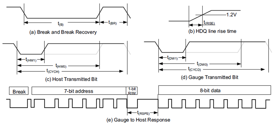 Figure 2. HDQ Timing
7.28 Typical Characteristics
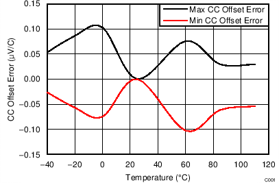
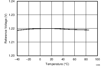
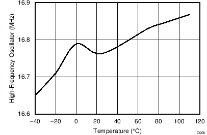
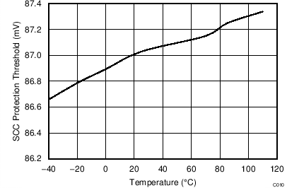
| Threshold setting is 25 mV. | ||

| Threshold setting is –177.7 mV. | ||
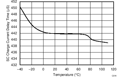
| Threshold setting is 465 µs. | ||
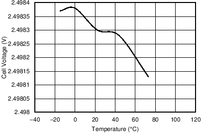
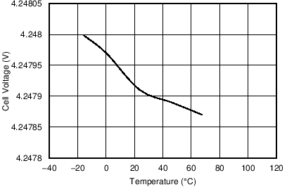
| This is the VCELL average for single cell. |
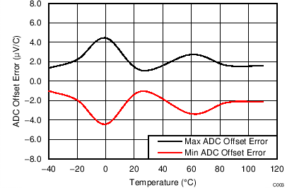
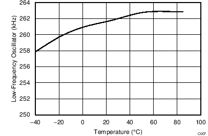
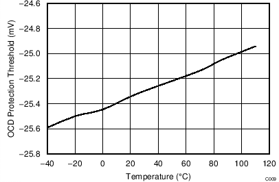
| Threshold setting is 25 mV. | ||
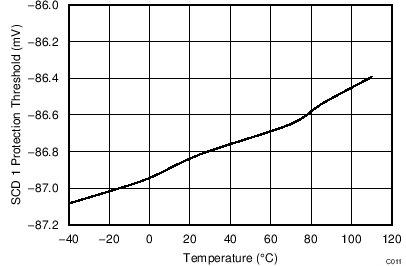
| Threshold setting is –88.85 mV. | ||

| Threshold setting is 11 ms. | ||
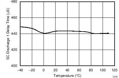
| Threshold setting is 465 µs (including internal delay). | ||
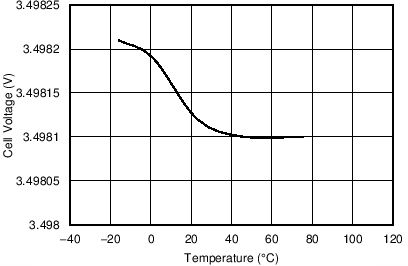
| This is the VCELL average for single cell. |
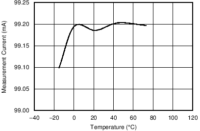
| ISET = 100 mA | ||