ZHCSG63C December 2013 – July 2018
PRODUCTION DATA.
- 1 特性
- 2 应用
- 3 说明
- 4 修订历史记录
- 5 Device Comparison Table
- 6 Pin Configuration and Functions
- 7 Specifications
-
8 Detailed Description
- 8.1 Overview
- 8.2 Functional Block Diagram
- 8.3
Feature Description
- 8.3.1 Details of a Qi Wireless Power System and bq51003 Power Transfer Flow Diagrams
- 8.3.2 Dynamic Rectifier Control
- 8.3.3 Dynamic Efficiency Scaling
- 8.3.4 RILIM Calculations
- 8.3.5 Input Overvoltage
- 8.3.6 Adapter Enable Functionality and EN1/EN2 Control
- 8.3.7 End Power Transfer Packet (WPC Header 0x02)
- 8.3.8 Status Outputs
- 8.3.9 WPC Communication Scheme
- 8.3.10 Communication Modulator
- 8.3.11 Adaptive Communication Limit
- 8.3.12 Synchronous Rectification
- 8.3.13 Temperature Sense Resistor Network (TS)
- 8.3.14 3-State Driver Recommendations for the TS-CTRL Pin
- 8.3.15 Thermal Protection
- 8.3.16 WPC v1.2 Compliance – Foreign Object Detection
- 8.4 Device Functional Modes
- 9 Application and Implementation
- 10Power Supply Recommendations
- 11Layout
- 12器件和文档支持
- 13机械、封装和可订购信息
8.3.9 WPC Communication Scheme
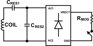
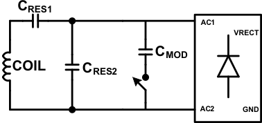
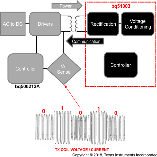
The WPC communication uses a modulation technique termed backscatter modulation where the receiver coil is dynamically loaded to provide amplitude modulation of the transmitter's coil voltage and current. This scheme is possible due to the fundamental behavior between two loosely coupled inductors (that is, between the Tx and Rx coil). This type of modulation can be accomplished by switching in and out a resistor at the output of the rectifier, or by switching in and out a capacitor across the AC1/AC2 net. Figure 20 shows how to implement resistive modulation.
 Figure 20. Resistive Modulation
 Figure 21 shows how to implement capacitive modulation.
 Figure 21. Capacitive Modulation
 The amplitude change in Tx coil voltage or current can be detected by the transmitters decoder. Figure 22 shows the resulting signal observed by the Tx.
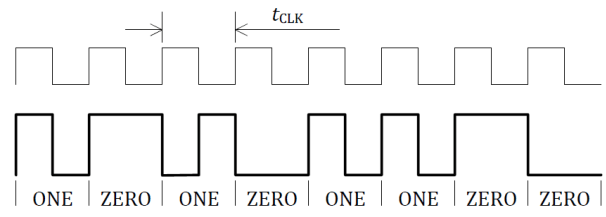
The WPC protocol uses a differential biphase encoding scheme to modulate the data bits onto the Tx coil voltage and current. Each data bit is aligned at a full period of 0.5 ms (tCLK) or 2 kHz. An encoded ONE results in two transitions during the bit period and an encoded ZERO results in a single transition. See Figure 23 for an example of the differential biphase encoding.
 Figure 23. Differential Biphase Encoding Scheme (WPC Volume 1: Low Power, Part 1 Interface Definition)
 The bits are sent LSB first and use an 11-bit asynchronous serial format for each portion of the packet. This includes one start bit, n-data bytes, a parity bit, and a single stop bit. The start bit is always ZERO and the parity bit is odd. The stop bit is always ONE. Figure 24 shows the details of the asynchronous serial format.
 Figure 24. Asynchronous Serial Formatting (WPC volume 1: Low Power, Part 1 Interface Definition)
 Each packet format is organized as shown in Figure 25.
 Figure 25. Packet Format (WPC Volume 1: Low Power, Part 1 Interface Definition)
 Figure 16 shows an example waveform of the receiver sending a rectified power packet (header 0x04).
