ZHCSAO7B December 2012 – June 2016
- 1 特性
- 2 应用范围
- 3 说明
- 4 修订历史记录
- 5 Pin Configuration and Functions
- 6 Specifications
-
7 Detailed Description
- 7.1 Overview
- 7.2 Functional Block Diagram
- 7.3
Feature Description
- 7.3.1 Dynamic Power Limiting™
- 7.3.2 Option Select Pin
- 7.3.3 LED Indication Modes
- 7.3.4 Parasitic Metal Object Detect (PMOD) and Foreign Object Detection (FOD)
- 7.3.5 Shut Down via External Thermal Sensor or Trigger
- 7.3.6 Fault Handling and Indication
- 7.3.7 Power Transfer Start Signal
- 7.3.8 Power-On Reset
- 7.3.9 External Reset, RESET Pin
- 7.3.10 Trickle Charge and CS100
- 7.3.11 Current Monitoring Requirements
- 7.3.12 Overcurrent Protection
- 7.3.13 MSP430G2001 Low Power Supervisor
- 7.3.14 All Unused Pins
- 8 Application and Implementation
- 9 Layout
- 10器件和文档支持
- 11机械、封装和可订购信息
6 Specifications
6.1 Absolute Maximum Ratings(1)
over operating free-air temperature range (unless otherwise noted)| MIN | MAX | UNIT | |
|---|---|---|---|
| Voltage applied at V33D to GND | –0.3 | 3.6 | V |
| Voltage applied at V33A to GND | –0.3 | 3.6 | |
| Voltage applied to any pin (2) | –0.3 | 3.6 | |
| Storage temperature,TSTG | –40 | 150 | °C |
(1) Stresses beyond those listed under Absolute Maximum Ratings may cause permanent damage to the device. These are stress ratings only, which do not imply functional operation of the device at these or any other conditions beyond those indicated under Recommended Operating Conditions. Exposure to absolute-maximum-rated conditions for extended periods may affect device reliability.
(2) All voltages referenced to GND.
6.2 Recommended Operating Conditions
over operating free-air temperature range (unless otherwise noted)| MIN | NOM | MAX | UNIT | ||
|---|---|---|---|---|---|
| V | Supply voltage during operation, V33D, V33A | 3.0 | 3.3 | 3.6 | V |
| TA | Operating free-air temperature range | –40 | 110 | °C | |
| TJ | Junction temperature | 110 | |||
6.3 Thermal Information
| THERMAL METRIC(1) | bq500211A | UNIT | |
|---|---|---|---|
| RGZ (VQFN) | |||
| 48 PINS | |||
| RθJA | Junction-to-ambient thermal resistance | 28.4 | °C/W |
| RθJC(top) | Junction-to-case (top) thermal resistance | 14.2 | °C/W |
| RθJB | Junction-to-board thermal resistance | 5.4 | °C/W |
| ψJT | Junction-to-top characterization parameter | 0.2 | °C/W |
| ψJB | Junction-to-board characterization parameter | 5.3 | °C/W |
| RθJC(bot) | Junction-to-case (bottom) thermal resistance | 1.4 | °C/W |
(1) For more information about traditional and new thermal metrics, see the Semiconductor and IC Package Thermal Metrics application report, SPRA953.
6.4 Electrical Characteristics
over operating free-air temperature range (unless otherwise noted)| PARAMETER | TEST CONDITIONS | MIN | TYP | MAX | UNIT | ||
|---|---|---|---|---|---|---|---|
| SUPPLY CURRENT | |||||||
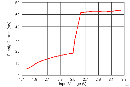
| IV33A | Supply current | V33A = 3.3 V | 8 | 15 | mA | ||
| IV33D | V33D = 3.3 V | 44 | 55 | ||||
| ITOTAL | V33D = V33A = 3.3 V | 52 | 60 | ||||
| INTERNAL REGULATOR CONTROLLER INPUTS/OUTPUTS | |||||||
| V33 | 3.3-V linear regulator | Emitter of NPN transistor | 3.25 | 3.3 | 3.6 | V | |
| V33FB | 3.3-V linear regulator feedback | 4 | 4.6 | ||||
| IV33FB | Series pass base drive | VIN = 12 V; current into V33FB pin | 10 | mA | |||
| Beta | Series NPN pass device | 40 | |||||
| EXTERNALLY SUPPLIED 3.3 V POWER | |||||||
| V33D | Digital 3.3-V power | TA = 25°C | 3 | 3.6 | V | ||
| V33A | Analog 3.3-V power | TA = 25°C | 3 | 3.6 | |||
| V33Slew | V33 slew rate | V33 slew rate between 2.3 V and 2.9 V, V33A = V33D |
0.25 | V/ms | |||
| DIGITAL DEMODULATION INPUTS COMM_A+, COMM_A-, COMM_B+, COMM_B- | |||||||
| VCM | Common mode voltage each pin | –0.15 | 1.631 | V | |||
| COMM+, COMM- | Modulation voltage digital resolution | 1 | mV | ||||
| REA | Input impedance | Ground reference | 0.5 | 1.5 | 3 | MΩ | |
| IOFFSET | Input offset current | 1-kΩ source impedance | –5 | 5 | µA | ||
| ANALOG INPUTS V_SENSE, I_SENSE, T_SENSE, LED_MODE | |||||||
| VADDR_OPEN | Voltage indicating open pin | LED_MODE open | 2.37 | V | |||
| VADDR_SHORT | Voltage indicating pin shorted to GND | LED_MODE shorted to ground | 0.36 | ||||
| VADC_RANGE | Measurement range for voltage monitoring | ALL ANALOG INPUTS | 0 | 2.5 | |||
| INL | ADC integral nonlinearity | –2.5 | 2.5 | mV | |||
| Ilkg | Input leakage current | 3 V applied to pin | 100 | nA | |||
| RIN | Input impedance | Ground reference | 8 | MΩ | |||
| CIN | Input capacitance | 10 | pF | ||||
| DIGITAL INPUTS/OUTPUTS | |||||||
| VOL | Low-level output voltage | IOL = 6 mA , V33D = 3 V | DGND1 + 0.25 | V | |||
| VOH | High-level output voltage | IOH = -6 mA , V33D = 3 V | V33D – 0.6V |
||||
| VIH | High-level input voltage | V33D = 3V | 2.1 | 3.6 | |||
| VIL | Low-level input voltage | V33D = 3.5 V | 1.4 | ||||
| IOH(MAX) | Output high source current | 4 | mA | ||||
| IOL(MAX) | Output low sink current | 4 | |||||
| SYSTEM PERFORMANCE | |||||||
| VRESET | Voltage where device comes out of reset | V33D Pin | 2.3 | 2.4 | V | ||
| tRESET | Pulse width needed for reset | RESET pin | 2 | µs | |||
| fSW | Switching Frequency | 112 | 205 | kHz | |||
| tdetect | Time to detect presence of device requesting power | 0.5 | s | ||||
| tretention | Retention of configuration parameters | TJ = 25°C | 100 | Years | |||
6.5 Typical Characteristics Curves

