ZHCSRC1 December 2022 BQ34Z100-R2
PRODUCTION DATA
- 1 特性
- 2 应用
- 3 说明
- 4 Revision History
- 5 Pin Configuration and Functions
-
6 Specifications
- 6.1 Absolute Maximum Ratings
- 6.2 ESD Ratings
- 6.3 Recommended Operating Conditions
- 6.4 Thermal Information
- 6.5 Electrical Characteristics: Power-On Reset
- 6.6 Electrical Characteristics: LDO Regulator
- 6.7 Electrical Characteristics: Internal Temperature Sensor Characteristics
- 6.8 Electrical Characteristics: Low-Frequency Oscillator
- 6.9 Electrical Characteristics: High-Frequency Oscillator
- 6.10 Electrical Characteristics: Integrating ADC (Coulomb Counter) Characteristics
- 6.11 Electrical Characteristics: ADC (Temperature and Cell Measurement) Characteristics
- 6.12 Electrical Characteristics: Data Flash Memory Characteristics
- 6.13 Timing Requirements: HDQ Communication
- 6.14 Timing Requirements: I2C-Compatible Interface
- 6.15 Typical Characteristics
- 7 Functional Block Diagram
-
8 Application and Implementation
- 8.1 Application Information
- 8.2
Typical Applications
- 8.2.1 Design Requirements
- 8.2.2
Detailed Design Procedure
- 8.2.2.1
Step-by-Step Design Procedure
- 8.2.2.1.1 STEP 1: Review and Modify the Data Flash Configuration Data.
- 8.2.2.1.2 STEP 2: Review and Modify the Data Flash Configuration Registers.
- 8.2.2.1.3 STEP 3: Design and Configure the Voltage Divider.
- 8.2.2.1.4 STEP 4: Determine the Sense Resistor Value.
- 8.2.2.1.5 STEP 5: Review and Modify the Data Flash Gas Gauging Configuration, Data, and State.
- 8.2.2.1.6 STEP 6: Determine and Program the Chemical ID.
- 8.2.2.1.7 STEP 7: Calibrate.
- 8.2.2.1.8 STEP 8: Run an Optimization Cycle.
- 8.2.2.1
Step-by-Step Design Procedure
- 9 Power Supply Recommendations
- 10Layout
- 11Device and Documentation Support
- 12Mechanical, Packaging, and Orderable Information
10.2.3 Board Offset Considerations
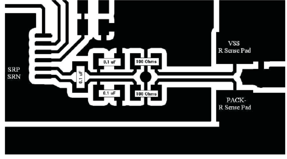
Although the most important component for board offset reduction is the decoupling capacitor for VCC, additional benefit is possible by using this recommended pattern for the coulomb counter differential low-pass filter network. Maintain the symmetrical placement pattern shown for optimum current offset performance. Use symmetrical shielded differential traces, if possible, from the sense resistor to the 100-Ω resistors, as shown in Figure 10-2.
 Figure 10-2 Differential Connection
Between SRP and SRN Pins with Sense Resistor