ZHCSBS5D January   2011  – May 2015

PRODUCTION DATA.  

  1. 特性
  2. 应用
  3. 说明
  4. 简化电路原理图
  5. 修订历史记录
  6. Pin Configuration and Functions
  7. Specifications
    1. 7.1  Absolute Maximum Ratings
    2. 7.2  ESD Ratings
    3. 7.3  Recommended Operating Conditions
    4. 7.4  Thermal Information
    5. 7.5  Electrical Characteristics: Supply Current
    6. 7.6  Power-On Reset (POR)
    7. 7.7  Wake From Sleep
    8. 7.8  RBI RAM Backup
    9. 7.9  3.3-V Regulator
    10. 7.10 2.5-V Regulator
    11. 7.11 DISP, PRES, SMBD, SMBC
    12. 7.12 CHG, DSG FET Drive
    13. 7.13 Internal Precharge Limiting
    14. 7.14 GPOD
    15. 7.15 FUSE
    16. 7.16 LED5, LED4, LED3, LED2, LED1
    17. 7.17 Coulomb Counter
    18. 7.18 VC1, VC2, VC3, VC4
    19. 7.19 TS1, TS2
    20. 7.20 Internal Temperature Sensor
    21. 7.21 Internal Thermal Shutdown
    22. 7.22 High-Frequency Oscillator
    23. 7.23 Low-Frequency Oscillator
    24. 7.24 Internal Voltage Reference
    25. 7.25 Flash
    26. 7.26 OCD Current Protection
    27. 7.27 SCD1 Current Protection
    28. 7.28 SCD2 Current Protection
    29. 7.29 SCC Current Protection
    30. 7.30 SBS Timing Requirements
    31. 7.31 Typical Characteristics
  8. Parameter Measurement Information
    1. 8.1 Battery Parameter Measurements
      1. 8.1.1 Charge and Discharge Counting
      2. 8.1.2 Voltage
      3. 8.1.3 Current
      4. 8.1.4 Auto Calibration
      5. 8.1.5 Temperature
      6. 8.1.6 Communications
        1. 8.1.6.1 SMBus On and Off State
        2. 8.1.6.2 SBS Commands
  9. Detailed Description
    1. 9.1 Overview
      1. 9.1.1 Configuration
        1. 9.1.1.1 Oscillator Function
        2. 9.1.1.2 System Present Operation
        3. 9.1.1.3 2-, 3-, or 4-Cell Configuration
        4. 9.1.1.4 Cell Balancing
          1. 9.1.1.4.1 Internal Cell Balancing
          2. 9.1.1.4.2 External Cell Balancing
    2. 9.2 Functional Block Diagram
    3. 9.3 Feature Description
      1. 9.3.1 Primary (1st Level) Safety Features
      2. 9.3.2 Secondary (2nd Level) Safety Features
      3. 9.3.3 Charge Control Features
      4. 9.3.4 Gas Gauging
      5. 9.3.5 Lifetime Data Logging Features
      6. 9.3.6 Authentication
    4. 9.4 Device Functional Modes
  10. 10Application and Implementation
    1. 10.1 Application Information
    2. 10.2 Typical Application
      1. 10.2.1 Design Requirements
      2. 10.2.2 Detailed Design Procedure
        1. 10.2.2.1 High-Current Path
          1. 10.2.2.1.1 Protection FETs
          2. 10.2.2.1.2 Chemical Fuse
          3. 10.2.2.1.3 Lithium-Ion Cell Connections
          4. 10.2.2.1.4 Sense Resistor
          5. 10.2.2.1.5 ESD Mitigation
        2. 10.2.2.2 Gas Gauge Circuit
          1. 10.2.2.2.1 Differential Low-Pass Filter
          2. 10.2.2.2.2 Power Supply Decoupling and RBI
          3. 10.2.2.2.3 System Present
          4. 10.2.2.2.4 SMBus Communication
          5. 10.2.2.2.5 FUSE Circuitry
          6. 10.2.2.2.6 PFIN Detection
        3. 10.2.2.3 Secondary-Current Protection
          1. 10.2.2.3.1 Cell and Battery Inputs
          2. 10.2.2.3.2 External Cell Balancing
          3. 10.2.2.3.3 PACK and FET Control
          4. 10.2.2.3.4 Regulator Output
          5. 10.2.2.3.5 Temperature Output
          6. 10.2.2.3.6 LEDs
          7. 10.2.2.3.7 Safety PTC Thermistor
        4. 10.2.2.4 Secondary-Overvoltage Protection
          1. 10.2.2.4.1 Cell Inputs
          2. 10.2.2.4.2 Time-Delay Capacitor
      3. 10.2.3 Application Curves
    3. 10.3 System Example
  11. 11Power Supply Recommendations
  12. 12Layout
    1. 12.1 Layout Guidelines
    2. 12.2 Layout Example
  13. 13器件和文档支持
    1. 13.1 文档支持
      1. 13.1.1 相关文档
    2. 13.2 社区资源
    3. 13.3 商标
    4. 13.4 Glossary
  14. 14机械、封装和可订购信息

封装选项

机械数据 (封装 | 引脚)
散热焊盘机械数据 (封装 | 引脚)
订购信息

12 Layout

12.1 Layout Guidelines

The predominant layout concern for the bq3050 is related to the coulomb counter measurement. The external components and PCB layout surrounding the SRP and SRN pins should be carefully considered.

12.2 Layout Example

As shown in Figure 26, a differential filter must precede the current sense inputs of the gas gauge. This filter eliminates the effect of unwanted digital noise, which can cause offset in the measured current. Even the best differential amplifier has less common-mode rejection at high frequencies. Without a filter, the amplifier input stage may rectify a strong RF signal, which then may appear as a DC-offset error.

Five percent tolerance of the components is adequate, because capacitor C15 shunts C12 and C13 and reduces AC common mode arising from a component mismatch. It is important to locate C15 as close as possible to the gas gauge pins. The other components also must be relatively close to the IC. The ground connection of C12 and C13 must be close to the IC. It is also proven to reduce offset and noise error by maintaining a symmetrical placement pattern and adding ground shielding for the differential filter network.
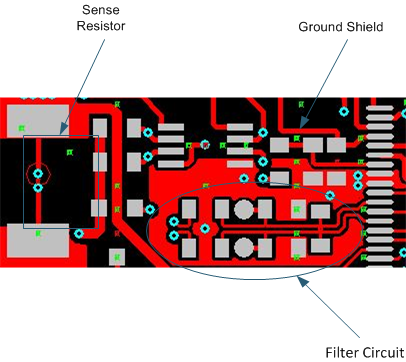
bq3050 SenseResistorLayout_3050.png Figure 26. PCB Layout Example