ZHCSDO4B May   2015  – May 2018

PRODUCTION DATA.  

  1. 特性
  2. 应用
  3. 说明
    1.     Device Images
      1.      简化原理图
  4. 修订历史记录
  5. Device Comparison Table
  6. Pin Configuration and Functions
    1.     Pin Functions
  7. Specifications
    1. 7.1  Absolute Maximum Ratings
    2. 7.2  ESD Ratings
    3. 7.3  Recommended Operating Conditions
    4. 7.4  Thermal Information
    5. 7.5  Supply Current
    6. 7.6  Digital Input and Output DC Characteristics
    7. 7.7  Power-On Reset
    8. 7.8  2.5-V LDO Regulator
    9. 7.9  Internal Clock Oscillators
    10. 7.10 Integrating ADC (Coulomb Counter) Characteristics
    11. 7.11 ADC (Temperature and Cell Voltage) Characteristics
    12. 7.12 Data Flash Memory Characteristics
    13. 7.13 HDQ Communication Timing Characteristics
    14. 7.14 I2C-Compatible Interface Timing Characteristics
    15. 7.15 Typical Characteristics
  8. Detailed Description
    1. 8.1 Overview
    2. 8.2 Functional Block Diagram
    3. 8.3 Feature Description
      1. 8.3.1 Fuel Gauging
      2. 8.3.2 Impedance Track Variables
      3. 8.3.3 Power Control
        1. 8.3.3.1 Reset Functions
        2. 8.3.3.2 Wake-Up Comparator
        3. 8.3.3.3 Flash Updates
      4. 8.3.4 Autocalibration
      5. 8.3.5 Communications
        1. 8.3.5.1 Authentication
        2. 8.3.5.2 Key Programming (Data Flash Key)
        3. 8.3.5.3 Key Programming (Secure Memory Key)
        4. 8.3.5.4 Executing an Authentication Query
        5. 8.3.5.5 HDQ Single-Pin Serial Interface
        6. 8.3.5.6 HDQ Host Interruption Feature
          1. 8.3.5.6.1 Low Battery Capacity
          2. 8.3.5.6.2 Temperature
        7. 8.3.5.7 I2C Interface
          1. 8.3.5.7.1 I2C Time Out
          2. 8.3.5.7.2 I2C Command Waiting Time
          3. 8.3.5.7.3 I2C Clock Stretching
    4. 8.4 Device Functional Modes
      1. 8.4.1 Power Modes
        1. 8.4.1.1 NORMAL Mode
        2. 8.4.1.2 SLEEP Mode
        3. 8.4.1.3 FULLSLEEP Mode
        4. 8.4.1.4 HIBERNATE Mode
      2. 8.4.2 System Control Function
        1. 8.4.2.1 SHUTDOWN Mode
        2. 8.4.2.2 INTERRUPT Mode
      3. 8.4.3 Security Modes
        1. 8.4.3.1 Sealing and Unsealing Data Flash
    5. 8.5 Programming
      1. 8.5.1 Standard Data Commands
        1. 8.5.1.1 Control(): 0x00 and 0x01
    6. 8.6 Register Maps
      1. 8.6.1 Pack Configuration Register
      2. 8.6.2 Pack Configuration B Register
      3. 8.6.3 Pack Configuration C Register
  9. Application and Implementation
    1. 9.1 Application Information
    2. 9.2 Typical Applications
      1. 9.2.1 Design Requirements
      2. 9.2.2 Detailed Design Procedure
        1. 9.2.2.1 BAT Voltage Sense Input
        2. 9.2.2.2 SRP and SRN Current Sense Inputs
        3. 9.2.2.3 Sense Resistor Selection
        4. 9.2.2.4 TS Temperature Sense Input
        5. 9.2.2.5 Thermistor Selection
        6. 9.2.2.6 REGIN Power Supply Input Filtering
        7. 9.2.2.7 VCC LDO Output Filtering
    3. 9.3 Application Curves
  10. 10Power Supply Recommendations
    1. 10.1 Power Supply Decoupling
  11. 11Layout
    1. 11.1 Layout Guidelines
      1. 11.1.1 Sense Resistor Connections
      2. 11.1.2 Thermistor Connections
      3. 11.1.3 High-Current and Low-Current Path Separation
    2. 11.2 Layout Example
  12. 12器件和文档支持
    1. 12.1 文档支持
      1. 12.1.1 相关文档
    2. 12.2 社区资源
    3. 12.3 商标
    4. 12.4 静电放电警告
    5. 12.5 术语表
  13. 13机械、封装和可订购信息

封装选项

机械数据 (封装 | 引脚)
散热焊盘机械数据 (封装 | 引脚)
订购信息

Application Curves

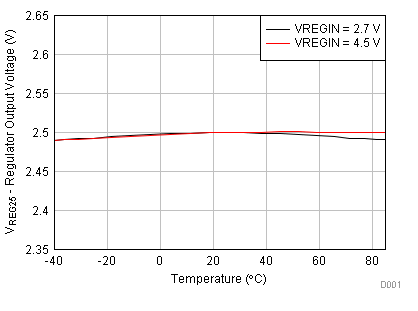
bq27546-G1 D001_SLUSBU6.gif
Figure 11. Regulator Output Voltage Vs. Temperature
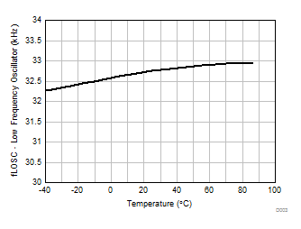
bq27546-G1 D003_SLUSBU6.gif
Figure 13. Low-Frequency Oscillator Frequency Vs. Temperature
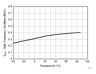
bq27546-G1 D002_SLUSBU6.gif
Figure 12. High-Frequency Oscillator Frequency Vs. Temperature
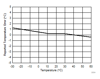
bq27546-G1 D004_SLUSBU6.gif
Figure 14. Reported Internal Temperature Measurement Vs. Temperature