ZHCSLT1B december 2020 – july 2023 BQ25672
PRODUCTION DATA
- 1
- 1 特性
- 2 应用
- 3 说明
- 4 Revision History
- 5 说明(续)
- 6 Pin Configuration and Functions
- 7 Specifications
-
8 Detailed Description
- 8.1 Overview
- 8.2 Functional Block Diagram
- 8.3
Feature Description
- 8.3.1 Device Power-On-Reset
- 8.3.2 PROG Pin Configuration
- 8.3.3 Device Power Up from Battery without Input Source
- 8.3.4 Device Power Up from Input Source
- 8.3.5 Dual-Input Power Mux
- 8.3.6 Buck Converter Operation
- 8.3.7 USB On-The-Go (OTG)
- 8.3.8 Power Path Management
- 8.3.9 Battery Charging Management
- 8.3.10 Integrated 16-Bit ADC for Monitoring
- 8.3.11 Status Outputs ( STAT, and INT)
- 8.3.12 Ship FET Control
- 8.3.13
Protections
- 8.3.13.1
Voltage and Current Monitoring
- 8.3.13.1.1 VAC Over-voltage Protection (VAC_OVP)
- 8.3.13.1.2 VBUS Over-voltage Protection (VBUS_OVP)
- 8.3.13.1.3 VBUS Under-voltage Protection (POORSRC)
- 8.3.13.1.4 System Over-voltage Protection (VSYS_OVP)
- 8.3.13.1.5 System Short Protection (VSYS_SHORT)
- 8.3.13.1.6 Battery Over-voltage Protection (VBAT_OVP)
- 8.3.13.1.7 Battery Over-current Protection (IBAT_OCP)
- 8.3.13.1.8 Input Over-current Protection (IBUS_OCP)
- 8.3.13.1.9 OTG Over-voltage Protection (OTG_OVP)
- 8.3.13.1.10 OTG Under-voltage Protection (OTG_UVP)
- 8.3.13.2 Thermal Regulation and Thermal Shutdown
- 8.3.13.1
Voltage and Current Monitoring
- 8.3.14 Serial Interface
- 8.4 Device Functional Modes
- 8.5 Register Map
- 9 Application and Implementation
- 10Power Supply Recommendations
- 11Layout
- 12Device and Documentation Support
- 13Mechanical, Packaging, and Orderable Information
8.3.9.5.1 JEITA Guideline Compliance in Charge Mode
To improve the safety of charging Li-ion batteries, the JEITA guideline was released on April 20, 2007. The guideline emphasized the importance of avoiding a high charge current and high charge voltage at certain low and high temperature ranges.
To initiate a charge cycle, the voltage on the TS pin must be within the VT1 to VT5 thresholds. If TS voltage exceeds the VT1-VT5 range, the controller suspends charging and waits until the battery temperature is within the T1 to T5 range. At cool temperature T1-T2, JEITA recommends to reduce the charge current to be lower than half of the charge current at normal temperature T2-T3. The charger register bits JEITA_ISETC[1:0] provide the charge current programmability at T1-T2, to be 20%, 40% or 100% of the charge current in the T2-T3 temperature range or charge suspend. At warm temperature T3-T5, JEITA recommends charge voltage less than 4.1V / cell. The charger register bits JEITA_VSET[2:0] provide the charge voltage programmability at T3-T5, to be with a voltage offset less than charge voltage in the T2-T3 temperature range or charge suspend.
Charging termination is still enabled (when EN_TERM = 1) at cool temperature T1-T2 and warm temperature T3-T5. The termination current remains the same in all different temperature ranges. In normal operation, battery charging terminates when the charge current is lower than the termination current, the battery voltage is higher than the battery recharge voltage and the charger is in the battery voltage CV regulation loop. When the temperature enters the T1-T2 or T3-T5 ranges, the charge current may reduce to 20% or 40% of that in the T2-T3 range, which might be lower than the termination current setting. If at this moment, the battery voltage is already higher than the battery recharge voltage and the charger is in the battery voltage CV regulation loop, the charger terminates charge.
In warm T3-T5 temperature range, the battery voltage regulation value become lower than that in the T2-T3 temperature range. If the battery voltage is already very close to the T2-T3 regulation value, the JEITA warm automatic regulation voltage reduction might cause a battery over-voltage (VBAT_OVP) fault.
In cool T1-T2 temperature range or warm T3-T5 temperature range, the charge current is different from that at the normal T2-T3 temperature range , the safety timer must be adjusted accordingly. The safety timer is suspended when the charge is suspended, and runs at half of the clock rate when the charge current is reduced to 20% or 40%, but stays the same when the charge current is unchanged.
One typical JEITA charging values are shown as the figure below, in which the blue real line is the default setting and the red dash line is the programmable options.
 Figure 8-11 TS Charging Values
The NTC monitoring on the battery temperature can be ignored by the charger if TS_IGNORE = 1. When the TS pin feedback is ignored, the charger considers the TS is always good for charging and OTG modes. The TS_STAT including TS_COLD_STAT, TS_COOL_STAT, TS_WARM_STAT and TS_HOT_STAT, always report 000 with TS_IGNORE = 1.
When TS_IGNORE = 0, the charger adjusts the charging profile based on the TS pin feedback information. When the battery temperature jumps from one temperature range to the other one, the associated TS status bits are updated accordingly. The TS flag bits are set for the temperature range for which the TS voltage is reporting, and an INT pulse is asserted to alert the host if TS_MASK is low. The FLAG and INT pulse can be individually masked by properly setting the associated mask bit, to prevent the INT pulse from alerting the host of battery temperature range changes.
The typical TS resistor network is illustrated in the figure below.
 Figure 8-12 TS Resistor Network
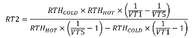
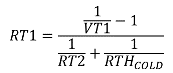
Assuming a 103AT NTC thermistor on the battery pack as shown above, the value of RT1 and RT2 can be determined by:
where VT# are the percentages of V(REGN) per the electrical specifications table. The BQ25672 provides the comparators with fixed thresholds for VT1 x V(REGN) and VT5 x V(REGN), and comparators with programmable thresholds for VT2 x V(REGN) and VT3 x V(REGN). The thresholds for VT2 x V(REGN) and VT3 x V(REGN) are controlled by TS_COOL[1:0] and TS_WARM[1:0]. This programmability gives more flexibility for the configuration of the JEITA profile. Select T1=0°C and T5=60°C for Li-ion or Li-polymer battery, the RT1 and RT2 are calculated to be 5.24KΩ and 30.31KΩ respectively.