ZHCSLT1B december 2020 – july 2023 BQ25672
PRODUCTION DATA
- 1
- 1 特性
- 2 应用
- 3 说明
- 4 Revision History
- 5 说明(续)
- 6 Pin Configuration and Functions
- 7 Specifications
-
8 Detailed Description
- 8.1 Overview
- 8.2 Functional Block Diagram
- 8.3
Feature Description
- 8.3.1 Device Power-On-Reset
- 8.3.2 PROG Pin Configuration
- 8.3.3 Device Power Up from Battery without Input Source
- 8.3.4 Device Power Up from Input Source
- 8.3.5 Dual-Input Power Mux
- 8.3.6 Buck Converter Operation
- 8.3.7 USB On-The-Go (OTG)
- 8.3.8 Power Path Management
- 8.3.9 Battery Charging Management
- 8.3.10 Integrated 16-Bit ADC for Monitoring
- 8.3.11 Status Outputs ( STAT, and INT)
- 8.3.12 Ship FET Control
- 8.3.13
Protections
- 8.3.13.1
Voltage and Current Monitoring
- 8.3.13.1.1 VAC Over-voltage Protection (VAC_OVP)
- 8.3.13.1.2 VBUS Over-voltage Protection (VBUS_OVP)
- 8.3.13.1.3 VBUS Under-voltage Protection (POORSRC)
- 8.3.13.1.4 System Over-voltage Protection (VSYS_OVP)
- 8.3.13.1.5 System Short Protection (VSYS_SHORT)
- 8.3.13.1.6 Battery Over-voltage Protection (VBAT_OVP)
- 8.3.13.1.7 Battery Over-current Protection (IBAT_OCP)
- 8.3.13.1.8 Input Over-current Protection (IBUS_OCP)
- 8.3.13.1.9 OTG Over-voltage Protection (OTG_OVP)
- 8.3.13.1.10 OTG Under-voltage Protection (OTG_UVP)
- 8.3.13.2 Thermal Regulation and Thermal Shutdown
- 8.3.13.1
Voltage and Current Monitoring
- 8.3.14 Serial Interface
- 8.4 Device Functional Modes
- 8.5 Register Map
- 9 Application and Implementation
- 10Power Supply Recommendations
- 11Layout
- 12Device and Documentation Support
- 13Mechanical, Packaging, and Orderable Information
8.3.8.2 Dynamic Power Management
To meet the maximum current limit in USB spec and avoid over loading the adapter, the device features Dynamic Power Management (DPM), which continuously monitors the input current and input voltage. When the input power at the VBUS pin is too low to support the load from SYS pin and the battery charge current from BAT pin, the charger engages either IINDPM to limit its current or VINDPM to prevent further reduction in VBUS pin voltage.
When the system voltage is regulated at VSYSMIN, the charger could be in trickle charge, pre-charge or fast charge stages, the SYS voltage drops lower than VSYSMIN, the VSYSMIN loop takes over and reduces the trickle charge, pre-charge or fast charge current, so that the SYS voltage remains at the VSYSMIN level.
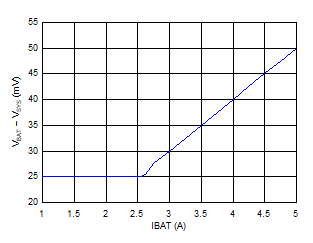
If the charge current falls to zero, but the input source is still overloaded, the SYS voltage will drop. Once the SYS voltage falls below the battery voltage, the device automatically enters Supplement Mode in which the BATFET turns on. The battery starts discharging so that the system is supported from both the input source and battery. In supplement mode, the battery FET is operated in ideal diode mode in which the charger regulates the battery FET gate voltage to keep the BATFET minimum VDS to approximately 25 mV when the current is low. This prevents SYS voltage oscillations from entering and exiting the supplement mode. As the discharge current increases, the charger regulates the BATFET gate to a higher voltage, in order to reduce the battery FET RDSON until the MOSFET is in full turn-on stage. At this point onwards, the VDS of the battery FET linearly increase with the discharge current. The figure below shows the V-I curve of the BATFET gate regulation operation. The BATFET turns off to exit Supplement Mode when the battery is below battery depletion threshold.
 Figure 8-8 BATFET I-V Curve
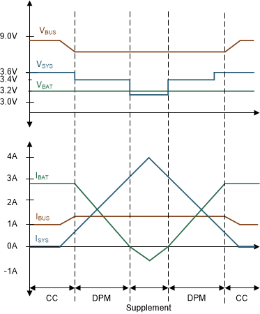
During DPM mode, the status register bits VINDPM_STAT (VINDPM) and/or IINDPM_STAT (IINDPM) go high. The figure below shows the DPM response with 9V/1.2A adapter, 3.2V battery, 2.8A charge current and 3.5V minimum system voltage setting.
 Figure 8-9 DPM Response