ZHCSKP6A January   2020  – February 2022 BQ25616

PRODUCTION DATA  

  1. 特性
  2. 应用
  3. 说明
  4. Revision History
  5. 说明(续)
  6. Device Comparison Table
  7. Pin Configuration and Functions
  8. Specifications
    1. 8.1 Absolute Maximum Ratings
    2. 8.2 ESD Ratings
    3. 8.3 Recommended Operating Conditions
    4. 8.4 Thermal Information
    5. 8.5 Electrical Characteristics
    6. 8.6 Timing Requirements
    7. 8.7 Typical Characteristics
  9. Detailed Description
    1. 9.1 Overview
    2. 9.2 Functional Block Diagram
    3. 9.3 Feature Description
      1. 9.3.1 Power-On-Reset (POR)
      2. 9.3.2 Device Power Up From Battery Without Input Source
      3. 9.3.3 Power Up From Input Source
        1. 9.3.3.1 Power Up ACFET
        2. 9.3.3.2 Power Up REGN LDO
        3. 9.3.3.3 Poor Source Qualification
        4. 9.3.3.4 Input Source Type Detection (IINDPM Threshold)
          1. 9.3.3.4.1 D+/D– Detection Sets Input Current Limit
        5. 9.3.3.5 Input Voltage Limit Threshold Setting (VINDPM Threshold)
        6. 9.3.3.6 Power Up Converter in Buck Mode
      4. 9.3.4 Boost Mode Operation From Battery
      5. 9.3.5 Standalone Charger
      6. 9.3.6 Power Path Management
        1. 9.3.6.1 Narrow VDC Architecture
        2. 9.3.6.2 Dynamic Power Management
        3. 9.3.6.3 Supplement Mode
      7. 9.3.7 Battery Charging Management
        1. 9.3.7.1 Autonomous Charging Cycle
        2. 9.3.7.2 Battery Charging Profile
        3. 9.3.7.3 Charging Termination
        4. 9.3.7.4 Thermistor Qualification
          1. 9.3.7.4.1 JEITA Guideline Compliance During Charging Mode (BQ25616J)
          2. 9.3.7.4.2 Hot/Cold Temperature Window During Charging Mode (BQ25616)
          3. 9.3.7.4.3 Boost Mode Thermistor Monitor During Battery Discharge Mode
        5. 9.3.7.5 Charging Safety Timer
      8. 9.3.8 Status Outputs ( PG, STAT)
        1. 9.3.8.1 Power Good Indicator ( PG Pin )
        2. 9.3.8.2 Charging Status Indicator (STAT)
      9. 9.3.9 Protections
        1. 9.3.9.1 Input Current Limit
        2. 9.3.9.2 Voltage and Current Monitoring in Buck Mode
          1. 9.3.9.2.1 Input Overvoltage Protection (ACOV)
          2. 9.3.9.2.2 System Overvoltage Protection (SYSOVP)
        3. 9.3.9.3 Voltage and Current Monitoring in Boost Mode
          1. 9.3.9.3.1 Boost Mode Overvoltage Protection
        4. 9.3.9.4 Thermal Regulation and Thermal Shutdown
          1. 9.3.9.4.1 Thermal Protection in Buck Mode
          2. 9.3.9.4.2 Thermal Protection in Boost Mode
        5. 9.3.9.5 Battery Protection
          1. 9.3.9.5.1 Battery Overvoltage Protection (BATOVP)
          2. 9.3.9.5.2 Battery Overdischarge Protection
          3. 9.3.9.5.3 System Overcurrent Protection
    4. 9.4 Device Functional Modes
  10. 10Application and Implementation
    1. 10.1 Application Information
    2. 10.2 Typical Applications
      1. 10.2.1 BQ25616/616J Application without External OVP
        1. 10.2.1.1 Design Requirements
        2. 10.2.1.2 Detailed Design Procedure
          1. 10.2.1.2.1 Inductor Selection
          2. 10.2.1.2.2 Input Capacitor and Resistor
          3. 10.2.1.2.3 Output Capacitor
        3. 10.2.1.3 Application Curves
      2. 10.2.2 BQ25616/616J Application with External OVP
        1. 10.2.2.1 Design Requirements
        2. 10.2.2.2 Detailed Design Procedure
        3. 10.2.2.3 Application Curves
  11. 11Power Supply Recommendations
  12. 12Layout
    1. 12.1 Layout Guidelines
    2. 12.2 Layout Example
  13. 13Device and Documentation Support
    1. 13.1 Device Support
      1. 13.1.1 第三方产品免责声明
    2. 13.2 Documentation Support
      1. 13.2.1 Related Documentation
    3. 13.3 接收文档更新通知
    4. 13.4 支持资源
    5. 13.5 Trademarks
    6. 13.6 Electrostatic Discharge Caution
    7. 13.7 术语表
  14. 14Mechanical, Packaging, and Orderable Information

封装选项

机械数据 (封装 | 引脚)
散热焊盘机械数据 (封装 | 引脚)
订购信息
Output Capacitor

Ensure that the output capacitance has enough ripple current rating to absorb the output switching ripple current. Equation 9 shows the output capacitor RMS current ICOUT calculation.

Equation 9. GUID-B90B49BD-6118-4D8B-BAC6-87CC08CAB558-low.gif

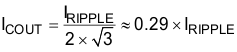
The output capacitor voltage ripple can be calculated as follows:

Equation 10. GUID-61B067DF-51B4-4849-AE50-0B76032051C7-low.gif

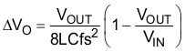
At certain input and output voltage and switching frequency, the voltage ripple can be reduced by increasing the output filter LC.

The charger device has internal loop compensation optimized for >10-μF ceramic output capacitance. The preferred ceramic capacitor is 10-V rating, X7R or X5R.