ZHCSMQ1A april 2020 – april 2021 BQ25170
PRODUCTION DATA
- 1
- 1 特性
- 2 应用
- 3 说明
- 4 Revision History
- 5 Pin Configuration and Functions
- 6 Specifications
- 7 Detailed Description
- 8 Application and Implementation
- 9 Power Supply Recommendations
- 10Layout
- 11Device and Documentation Support
- 12Mechanical, Packaging, and Orderable Information
请参考 PDF 数据表获取器件具体的封装图。
机械数据 (封装 | 引脚)
- DSG|8
散热焊盘机械数据 (封装 | 引脚)
7.3.2.4 Battery Cold, Hot Temperature Qualification (TS Pin)
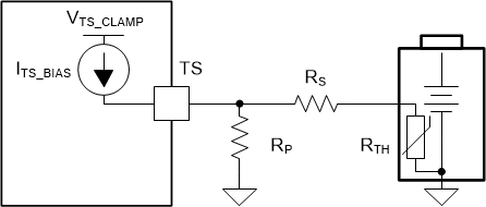
While charging, the device continuously monitors battery temperature by sensing the voltage at the TS pin. A negative temperature coefficient (NTC) thermistor should be connected between the TS and GND pins (recommend: 103AT-2). If temperature sensing is not required in the application, connect a fixed 10-kΩ resistor from TS to GND to allow normal operation. Battery charging is allowed when the TS pin voltage falls between VCOLD and VHOT thresholds (typically 0°C – 45°C). The temperature corresponding to these voltage thresholds can be modified by adding resistors in parallel and in series with the thermistor, as shown in Figure 7-3. If the TS pin indicates battery temperature is outside this range, the device stops charging, enters the STANDBY state, and blinks the STAT pin. Once battery temperature returns to normal conditions, charging resumes automatically.
 Figure 7-3 TS Resistor Network For Modified Temperature
Charging Window
Figure 7-3 TS Resistor Network For Modified Temperature
Charging Window| TEMPERATURE CHARGING WINDOW | RS | RP |
|---|---|---|
| 0°C to 60°C | 1.9 kΩ | 400 kΩ |
| −10°C to 60°C | 2.3 kΩ | 70 kΩ |
| −10°C to 50°C | 1.1 kΩ | 70 kΩ |
In addition to battery temperature sensing, the TS pin can be used to disable the charger at any time by pulling TS voltage below VTS_ENZ. The device disables the charger and consumes ISD_IN_TS from the input supply. In order to minimize quiescent current, the TS current source (ITS_BIAS) is duty-cycled, with an on-time of tTS_DUTY_ON and an off time of tTS_DUTY_OFF. After the TS pin pull-down is released, the device may take up to tTS_DUTY_OFF to turn the ITS_BIAS back on. After the source is turned on, the TS pin voltage will go above VTS_EN, and re-enable the charger operation. The device treats this TS pin toggle as an input supply toggle, triggering Device Power Up From Input Source (Section 7.3.1).