ZHCSJD3C july   2018  – april 2023 BQ25150

PRODUCTION DATA  

  1.   1
  2. 特性
  3. 应用
  4. 说明
  5. Revision History
  6. 说明(续)
  7. Device Key Default Settings
  8. Pin Configuration and Functions
  9. Specifications
    1. 8.1 Absolute Maximum Ratings
    2. 8.2 ESD Ratings
    3. 8.3 Recommended Operating Conditions
    4. 8.4 Thermal Information
    5. 8.5 Electrical Characteristics
    6. 8.6 Timing Requirements
    7. 8.7 Typical Characteristics
  10. Detailed Description
    1. 9.1 Overview
    2. 9.2 Functional Block Diagram
    3. 9.3 Feature Description
      1. 9.3.1  Linear Charger and Power Path
        1. 9.3.1.1 Battery Charging Process
          1. 9.3.1.1.1 Pre-Charge
          2. 9.3.1.1.2 Fast Charge
          3. 9.3.1.1.3 Pre-Charge to Fast Charge Transitions and Charge Current Ramping
          4. 9.3.1.1.4 Termination
        2. 9.3.1.2 JEITA and Battery Temperature Dependent Charging
        3. 9.3.1.3 Input Voltage Based Dynamic Power Management (VINDPM) and Dynamic Power Path Management (DPPM)
        4. 9.3.1.4 Battery Supplement Mode
      2. 9.3.2  Protection Mechanisms
        1. 9.3.2.1 Input Over-Voltage Protection
        2. 9.3.2.2 Safety Timer and I2C Watchdog Timer
        3. 9.3.2.3 Thermal Protection and Thermal Charge Current Foldback
        4. 9.3.2.4 Battery Short and Over Current Protection
        5. 9.3.2.5 PMID Short Circuit
        6. 9.3.2.6 Maximum Allowable Charging Current (IMAX)
      3. 9.3.3  ADC
        1. 9.3.3.1 ADC Operation in Active Battery Mode and Low Power Mode
        2. 9.3.3.2 ADC Operation When VIN Present
        3. 9.3.3.3 ADC Measurements
        4. 9.3.3.4 ADC Programmable Comparators
      4. 9.3.4  VDD LDO
      5. 9.3.5  Load Switch / LDO Output and Control
      6. 9.3.6  PMID Power Control
      7. 9.3.7  MR Wake and Reset Input
        1. 9.3.7.1 MR Wake or Short Button Press Functions
        2. 9.3.7.2 MR Reset or Long Button Press Functions
      8. 9.3.8  14-Second Watchdog for HW Reset
      9. 9.3.9  Faults Conditions and Interrupts ( INT)
        1. 9.3.9.1 Flags and Fault Condition Response
      10. 9.3.10 Power Good ( PG) Pin
      11. 9.3.11 External NTC Monitoring (TS)
        1. 9.3.11.1 TS Thresholds
      12. 9.3.12 External NTC Monitoring (ADCIN)
      13. 9.3.13 I2C Interface
        1. 9.3.13.1 F/S Mode Protocol
    4. 9.4 Device Functional Modes
      1. 9.4.1 Ship Mode
      2. 9.4.2 Low Power
      3. 9.4.3 Active Battery
      4. 9.4.4 Charger/Adapter Mode
      5. 9.4.5 Power-Up/Down Sequencing
    5. 9.5 Register Map
      1. 9.5.1 I2C Registers
  11. 10Application and Implementation
    1. 10.1 Application Information
    2. 10.2 Typical Application
      1. 10.2.1 Design Requirements
      2. 10.2.2 Detailed Design Procedure
        1. 10.2.2.1 Input (IN/PMID) Capacitors
        2. 10.2.2.2 VDD, LDO Input and Output Capacitors
        3. 10.2.2.3 TS
        4. 10.2.2.4 IMAX Selection
        5. 10.2.2.5 Recommended Passive Components
      3. 10.2.3 Application Curves
  12. 11Power Supply Recommendations
  13. 12Layout
    1. 12.1 Layout Guidelines
    2. 12.2 Layout Example
  14. 13Device and Documentation Support
    1. 13.1 Device Support
      1. 13.1.1 第三方产品免责声明
    2. 13.2 Documentation Support
      1. 13.2.1 Related Documentation
    3. 13.3 接收文档更新通知
    4. 13.4 支持资源
    5. 13.5 Trademarks
    6. 13.6 静电放电警告
    7. 13.7 术语表
  15. 14Mechanical, Packaging, and Orderable Information

封装选项

机械数据 (封装 | 引脚)
散热焊盘机械数据 (封装 | 引脚)
订购信息

Thermal Protection and Thermal Charge Current Foldback

During operation, to protect the device from damage due to overheating, the junction temperature of the die, TJ, is monitored. When TJ reaches TSHUTDOWN the device stops operation and is turned off. The device resumes operation when TJ falls below TSHUTDOWN by THYS.

During the charging process, to prevent overheating in the device, the device monitors the junction temperature of the die and reduces the charging current at a rate of (0.04 x ICHARGE )/°C once TJ exceeds the thermal foldback threshold, TREG. If the charge current is reduced to 0, the battery supplies the current needed to supply the PMID output. The thermal regulation threshold may be set through I2C by setting the THERM_REG bits to the desired value.

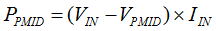
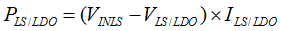
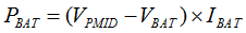
To ensure that the system power dissipation is under the limits of the device. The power dissipated by the device can be calculated using Equation 1:
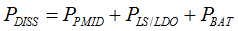
Equation 1. GUID-6241F306-CE9B-4502-8280-BA4FB97F68FE-low.gif

Where:

Equation 2. GUID-01C9C8A9-CFD7-4F5E-A219-17C0A31A8FDB-low.gif
Equation 3. GUID-C71F3F44-3F7E-4846-8454-3176F1A87BC7-low.gif
Equation 4. GUID-C752FB78-1213-4D10-91FB-A301A739E8F1-low.gif

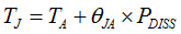
The die junction temperature, TJ, can be estimated based on the expected board performance using the following equation:

Equation 5. GUID-26C3E36C-0B17-4FF9-AC65-64EA7029415C-low.gif

The θJA is largely driven by the board layout. For more information about traditional and new thermal metrics, see the Semiconductor and IC Package Thermal Metrics Application Report. Under typical conditions, the time spent in this state is very short.