ZHCSI47A april 2018 – january 2021 BQ25121A
PRODUCTION DATA
- 1
- 1 特性
- 2 应用
- 3 说明
- 4 Revision History
- 5 Description (continued)
- 6 Device Comparison Table
- 7 Pin Configuration and Functions
- 8 Specifications
-
9 Detailed Description
- 9.1 Overview
- 9.2 Functional Block Diagram
- 9.3
Feature Description
- 9.3.1 Ship Mode
- 9.3.2 High Impedance Mode
- 9.3.3 Active Battery Only Connected
- 9.3.4 Voltage Based Battery Monitor
- 9.3.5 Sleep Mode
- 9.3.6 Input Voltage Based Dynamic Power Management (VIN(DPM))
- 9.3.7 Input Overvoltage Protection and Undervoltage Status Indication
- 9.3.8 Battery Charging Process and Charge Profile
- 9.3.9 Dynamic Power Path Management Mode
- 9.3.10 Battery Supplement Mode
- 9.3.11 Default Mode
- 9.3.12 Termination and Pre-Charge Current Programming by External Components (IPRETERM)
- 9.3.13 Input Current Limit Programming by External Components (ILIM)
- 9.3.14 Charge Current Programming by External Components (ISET)
- 9.3.15 Safety Timer
- 9.3.16 External NTC Monitoring (TS)
- 9.3.17 Thermal Protection
- 9.3.18 Typical Application Power Dissipation
- 9.3.19 Status Indicators ( PG and INT)
- 9.3.20 Chip Disable ( CD)
- 9.3.21 Buck (PWM) Output
- 9.3.22 Load Switch / LDO Output and Control
- 9.3.23 Manual Reset Timer and Reset Output ( MR and RESET)
- 9.4 Device Functional Modes
- 9.5 Programming
- 9.6
Register Maps
- 9.6.1 Status and Ship Mode Control Register
- 9.6.2 Faults and Faults Mask Register
- 9.6.3 TS Control and Faults Masks Register
- 9.6.4 Fast Charge Control Register
- 9.6.5 Termination/Pre-Charge Register
- 9.6.6 Battery Voltage Control Register
- 9.6.7 SYS VOUT Control Register
- 9.6.8 Load Switch and LDO Control Register
- 9.6.9 Push-button Control Register
- 9.6.10 ILIM and Battery UVLO Control Register
- 9.6.11 Voltage Based Battery Monitor Register
- 9.6.12 VIN_DPM and Timers Register
- 10Application and Implementation
- 11Power Supply Recommendations
- 12Layout
- 13Device and Documentation Support
- 14Mechanical, Packaging, and Orderable Information
9.3.16 External NTC Monitoring (TS)
The I2C interface allows the user to easily implement the JEITA standard for systems where the battery pack thermistor is monitored by the host. Additionally, the device provides a flexible voltage based TS input for monitoring the battery pack NTC thermistor. The voltage at TS is monitored to determine that the battery is at a safe temperature during charging.
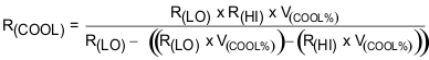
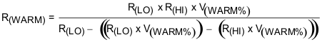
To satisfy the JEITA requirements, four temperature thresholds are monitored: the cold battery threshold, the cool battery threshold, the warm battery threshold, and the hot battery threshold. These temperatures correspond to the V(COLD), V(COOL), V(WARM), and V(HOT) threshold in Section 8.5. Charging and timers are suspended when V(TS) < V(HOT) or > V(COLD). When V(COOL) < V(TS) < V(COLD), the charging current is reduced to half of the programmed charge current. When V(HOT) < V(TS) < V(WARM), the battery regulation voltage is reduced by 140 mV (minimum VBATREG under this condition is 3.6V).
The TS function is voltage based for maximum flexibility. Connect a resistor divider from VIN to GND with TS connected to the center tap to set the threshold. The connections are shown in Figure 9-4. The resistor values are calculated using Equation 1 and Equation 2. To disable the TS function, pull TS above TSOFF threshold.
 Figure 9-4 TS
Circuit
Figure 9-4 TS
Circuit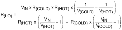
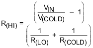
Where
- R(HOT) = the NTC resistance at the hot temperature
- R(COLD) = the NTC resistance at the cold temperature
The warm and cool thresholds are not independently programmable. The cool and warm NTC resistances for a selected resistor divider are calculated using Equation 3 and Equation 4.