ZHCSE30C August   2015  – September 2016 BQ25120 , BQ25121

PRODUCTION DATA.  

  1. 特性
  2. 应用
  3. 说明
    1.     简化原理图
  4. 修订历史记录
  5. 说明 (续)
  6. Device Comparison Table
  7. Pin Configuration and Functions
    1.     Pin Functions
  8. Specifications
    1. 8.1 Absolute Maximum Ratings
    2. 8.2 ESD Ratings
    3. 8.3 Recommended Operating Conditions
    4. 8.4 Thermal Information
    5. 8.5 Electrical Characteristics
    6. 8.6 Timing Requirements
    7. 8.7 Typical Characteristics
  9. Detailed Description
    1. 9.1 Overview
    2. 9.2 Functional Block Diagram
    3. 9.3 Feature Description
      1. 9.3.1  Ship Mode
      2. 9.3.2  High Impedance Mode
      3. 9.3.3  Active Battery Only Connected
      4. 9.3.4  Voltage Based Battery Monitor
      5. 9.3.5  Sleep Mode
      6. 9.3.6  Input Voltage Based Dynamic Power Management (VIN(DPM))
      7. 9.3.7  Input Overvoltage Protection and Undervoltage Status Indication
      8. 9.3.8  Battery Charging Process and Charge Profile
      9. 9.3.9  Dynamic Power Path Management Mode
      10. 9.3.10 Battery Supplement Mode
      11. 9.3.11 Default Mode
      12. 9.3.12 Termination and Pre-Charge Current Programming by External Components (IPRETERM)
      13. 9.3.13 Input Current Limit Programming by External Components (ILIM)
      14. 9.3.14 Charge Current Programming by External Components (ISET)
      15. 9.3.15 Safety Timer and Watchdog Timer
      16. 9.3.16 External NTC Monitoring (TS)
      17. 9.3.17 Thermal Protection
      18. 9.3.18 Typical Application Power Dissipation
      19. 9.3.19 Status Indicators (PG and INT)
      20. 9.3.20 Chip Disable (CD)
      21. 9.3.21 Buck (PWM) Output
      22. 9.3.22 Load Switch / LDO Output and Control
      23. 9.3.23 Manual Reset Timer and Reset Output (MR and RESET)
    4. 9.4 Device Functional Modes
    5. 9.5 Programming
      1. 9.5.1 Serial Interface Description
      2. 9.5.2 F/S Mode Protocol
    6. 9.6 Register Maps
      1. 9.6.1  Status and Ship Mode Control Register
        1. Table 12. Status and Ship Mode Control Register
      2. 9.6.2  Faults and Faults Mask Register
        1. Table 13. Faults and Faults Mask Register
      3. 9.6.3  TS Control and Faults Masks Register
        1. Table 14. TS Control and Faults Masks Register, Memory Location 0010
      4. 9.6.4  Fast Charge Control Register
        1. Table 15. Fast Charge Control Register
      5. 9.6.5  Termination/Pre-Charge and I2C Address Register
        1. Table 16. Termination/Pre-Charge and I2C Address Register
      6. 9.6.6  Battery Voltage Control Register
        1. Table 17. Battery Voltage Control Register
      7. 9.6.7  SYS VOUT Control Register
        1. Table 18. SYS VOUT Control Register
      8. 9.6.8  Load Switch and LDO Control Register
        1. Table 20. Load Switch and LDO Control Register
      9. 9.6.9  Push-button Control Register
        1. Table 21. Push-button Control Register
      10. 9.6.10 ILIM and Battery UVLO Control Register
        1. Table 22. ILIM and Battery UVLO Control Register, Memory Location 1001
      11. 9.6.11 Voltage Based Battery Monitor Register
        1. Table 23. Voltage Based Battery Monitor Register, Memory Location 1010
      12. 9.6.12 VIN_DPM and Timers Register
        1. Table 24. VIN_DPM and Timers Register
  10. 10Application and Implementation
    1. 10.1 Application Information
    2. 10.2 Typical Application
      1. 10.2.1 Design Requirements
      2. 10.2.2 Detailed Design Procedure
        1. 10.2.2.1 Default Settings
        2. 10.2.2.2 Choose the Correct Inductance and Capacitance
        3. 10.2.2.3 Calculations
          1. 10.2.2.3.1 Program the Fast Charge Current (ISET)
          2. 10.2.2.3.2 Program the Input Current Limit (ILIM)
          3. 10.2.2.3.3 Program the Pre-charge/termination Threshold (IPRETERM)
          4. 10.2.2.3.4 TS Resistors (TS)
      3. 10.2.3 Application Performance Curves
        1. 10.2.3.1 Charger Curves
        2. 10.2.3.2 SYS Output Curves
        3. 10.2.3.3 Load Switch and LDO Curves
        4. 10.2.3.4 LS/LDO Output Curves
        5. 10.2.3.5 Timing Waveforms Curves
  11. 11Power Supply Recommendations
  12. 12Layout
    1. 12.1 Layout Guidelines
    2. 12.2 Layout Example
  13. 13器件和文档支持
    1. 13.1 器件支持
      1. 13.1.1 第三方产品免责声明
    2. 13.2 相关链接
    3. 13.3 接收文档更新通知
    4. 13.4 社区资源
    5. 13.5 商标
    6. 13.6 静电放电警告
    7. 13.7 Glossary
  14. 14机械、封装和可订购信息

封装选项

机械数据 (封装 | 引脚)
散热焊盘机械数据 (封装 | 引脚)
订购信息

Device Functional Modes

Table 10. Modes and Functions

FUNCTION READY (PRIOR TO I2C) AND AFTER RESET HOST MODE READY (AFTER I2C) CHARGE SHIP MODE HIGH_Z ACTIVE BATTERY
VOVP Yes Yes Yes No No No
VUVLO Yes Yes Yes Yes Yes Yes
VBATUVLO Yes Yes Yes No Yes Yes
VINDPM OTP or registers OTP or registers If enabled No No No
SYS OTP or registers OTP or registers If enabled No If enabled If enabled
LS/LDO OTP or registers OTP or registers If enabled No If enabled If enabled
BATFET Yes Yes Yes No Yes Yes
TS Yes (VIN Valid) Yes (VIN Valid) Yes No No No
IPRETERM External OTP, registers, or external OTP, registers, or external No No No
ISET External OTP, registers, or external OTP, registers, or external No No No
ILIM External OTP, registers, or external OTP, registers, or external No No No
MR input Yes Yes Yes Yes Yes Yes
LSCTRL input Yes Yes Yes No Yes Yes
RESET output Yes Yes Yes No Yes Yes
INT output Yes Yes Yes No No Yes
I2C interface Yes Yes Yes No No Yes
CD input Yes Yes Yes No Yes Yes
PG output Yes Yes Yes No No If enabled
VBMON No Yes No No No Yes

Table 11. Fault and Status Condition Responses
FAULT or STATUS ACTIONS CHARGER BEHAVIOR SYS BEHAVIOR LS/LDO BEHAVIOR TS BEHAVIOR
VIN_OV Update VIN_OV status, Update STAT to fault, interrupt on INT, PG shown not good Disabled Enabled through BAT Enabled through BAT Disabled
VIN_UV Update VIN_UV status, Update STAT to fault, interrupt on INT, PG shown not good Disabled Enabled through BAT Enabled through BAT Disabled
VIN_ILIM Update charge in progress status, interrupt on INT, input current is limited Enabled, input current limited Enabled (if enabled) Enabled (if enabled) Enabled
OVER_TEMP Disabled Disabled Disabled Disabled
BAT_UVLO Update BAT_UVLO status, Update STAT to fault, interrupt on INT Pre-charge Enabled (if enabled) and VIN Valid Enabled (if enabled) and VIN Valid Enabled if VIN Valid
SW_SYS_SHORT Enabled Current Limit Enabled (if enabled) Enabled
LS_LDO_OCP Enabled Enabled (if enabled) Current Limit Enabled
TIMER fault Update TIMER, Update STAT to fault, interrupt on INT Disabled Enabled (if enabled) Enabled (if enabled) Disabled
VINDPM Update VINDPM_STAT, Update STAT to fault, interrupt on INT Enabled, input current reduced Enabled (if enabled) Enabled (if enabled) Enabled
TS_FAULT COLD or HOT Update TS_FAULT to COLD OR HOT, Update STAT to fault, interrupt on INT Disabled Enabled (if enabled) Enabled (if enabled) Enabled
TS_FAULT COOL Update TS_FAULT to COOL, Update STAT to fault, interrupt on INT Reduce ICHG to ½ Enabled (if enabled) Enabled (if enabled) Enabled
TS_FAULT WARM Update TS_FAULT to WARM, Update STAT to fault, interrupt on INT Reduce VBATREG by 140 mV Enabled (if enabled) Enabled (if enabled) Enabled
Charge Done Update STAT to Charge Done, interrupt on INT Disabled, monitor for VBAT falling below VRCHG Enabled (if enabled) Enabled (if enabled) Enabled
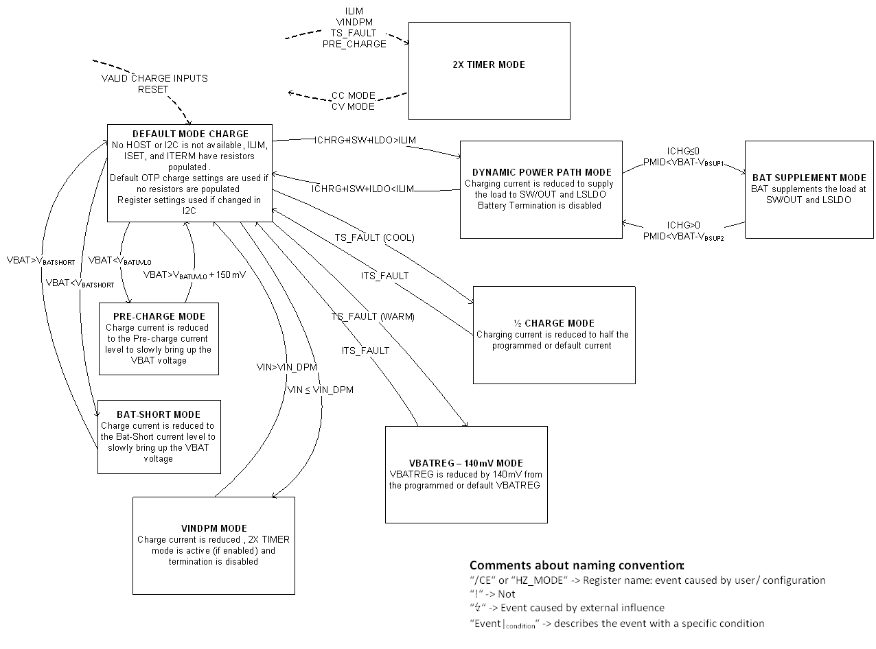
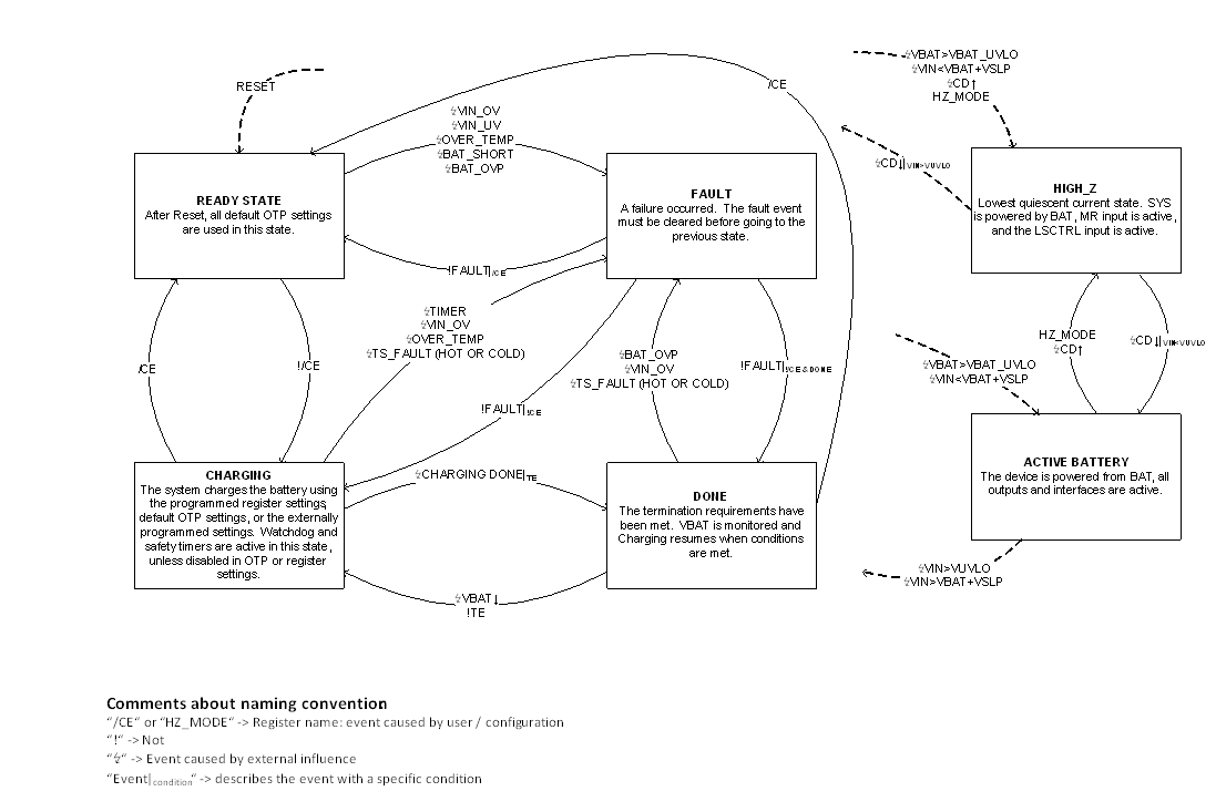
BQ25120 BQ25121 state_diagram_slusbz9.gifFigure 17. State Diagram
BQ25120 BQ25121 change_state_diagram_slusbz9.gifFigure 18. Change State Diagram