ZHCSCP0 July 2014
PRODUCTION DATA.
- 1 特性
- 2 应用范围
- 3 说明
- 4 应用电路原理图
- 5 修订历史记录
- 6 Device Comparison Table
- 7 Pin Configuration and Functions
- 8 Specifications
- 9 Detailed Description
- 10Application and Implementation
- 11Power Supply Recommendations
- 12Layout
- 13器件和文档支持
- 14机械封装和可订购信息
7 Pin Configuration and Functions
bq25071
(TOP VIEW)
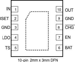
Pin Functions
| PIN | I/O | DESCRIPTION | |
|---|---|---|---|
| NAME | NO. | ||
| IN | 1 | I | Input power supply. IN is connected to the external DC supply (AC adapter or USB port). Bypass IN to GND with at least a 0.1 μF ceramic capacitor. |
| ISET | 2 | O | Input current programming bias pin. Connect a resistor from ISET to GND to program the input current limit when the user programmable mode is selected by grounding the EN pin. The resistor range is between 1 kΩ and 10 kΩ to set the current between 100 mA and 1 A. |
| GND | 3, 9 | – | Ground pin. Connect to the thermal pad and the ground plane of the circuit. |
| LDO | 4 | O | LDO output. LDO is regulated to 4.9V and drives up to 50 mA. Bypass LDO to GND with a 0.1 μF ceramic capacitor. LDO is enabled when V(UVLO) < VIN < V(OVP). |
| TS | 5 | I | Battery pack NTC monitoring input. Connect a resistor divider from LDO to GND with TS connected to the center tap to set the charge temperature window. The battery pack NTC is connected in parallel with the bottom resistor of the divider. See the Detailed Design Procedure section for details on the selecting the proper component values. |
| BAT | 6 | I | BAT is the sense input for the battery voltage. Connect BAT and OUT to the battery. |
| EN | 7 | I | Enable input. Drive EN high to disable the IC. Connect EN to GND to place the bq25071 in the user programmable mode using the ISET input where the input current is programmed. Leave EN floating to place the bq25071 in USB500 mode. See the Input Current Limit Control (EN) section for details on using the EN interface. |
| CHG | 8 | O | Charge status indicator open-drain output. CHG is pulled low while the device is charging the battery. CHG goes high impedance when the battery is fully charged. |
| OUT | 10 | O | System output connection. Bypass the OUT to GND with a 1 μF ceramic capacitor. Connect OUT and BAT together. |
| Thermal Pad | Pad | – | There is an internal electrical connection between the exposed thermal pad and the GND pin of the device. The thermal pad must be connected to the same potential as the GND pin on the printed circuit board. Do not use the thermal pad as the primary ground input for the device. GND pin must be connected to ground at all times. |