ZHCSCP0 July 2014
PRODUCTION DATA.
- 1 特性
- 2 应用范围
- 3 说明
- 4 应用电路原理图
- 5 修订历史记录
- 6 Device Comparison Table
- 7 Pin Configuration and Functions
- 8 Specifications
- 9 Detailed Description
- 10Application and Implementation
- 11Power Supply Recommendations
- 12Layout
- 13器件和文档支持
- 14机械封装和可订购信息
10 Application and Implementation
10.1 Application Information
The typical application circuit uses a single output which charges the battery and powers the system. Additionally a 50-mA LDO can supply a low power external circuit.
The bq25071EVM-658 evaluation module (EVM) is a complete charger module for evaluating the bq25071. Refer to SLUUB49.
10.2 Typical Application
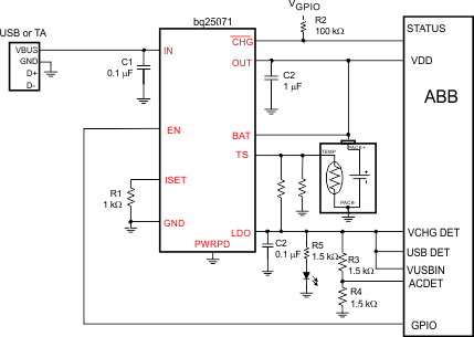 Figure 9. bq25071 Typical Application Circuit
10.2.1 Design Requirements
Table 2. Design Parameters
| PARAMETER | EXAMPLE VALUE |
|---|---|
| Input supply range | 5 V ±5% |
| Output voltage range | 3.5 V |
| Output current rating | 1000 mA |
10.2.2 Detailed Design Procedure
10.2.2.1 Selection of Input and Output Capacitors
In most applications, all that is needed is a high-frequency decoupling capacitor on the input power pin. For normal charging applications, a 0.1 μF ceramic capacitor, placed in close proximity to the IN pin and GND pad works best. In some applications, depending on the power supply characteristics and cable length, it may be necessary to increase the input filter capacitor to avoid exceeding the OVP voltage threshold during adapter hot plug events where the ringing exceeds the deglitch time.
The charger in the bq25071 requires a capacitor from OUT to GND for loop stability. Connect a 1 μF ceramic capacitor from OUT to GND close to the pins for best results. More output capacitance may be required to minimize the output drop during large load transients.
The LDO also requires an output capacitor for loop stability. Connect a 0.1 μF ceramic capacitor from LDO to GND close to the pins. For improved transient response, this capacitor may be increased.
10.2.2.2 Thermal Considerations
The bq25071 is packaged in a thermally enhanced QFN package. The package includes a thermal pad to provide an effective thermal contact between the IC and the printed circuit board (PCB). Full PCB design guidelines for this package are provided in the application note entitled: QFN/SON PCB Attachment Application Note (SLUA271).
The most common measure of package thermal performance is thermal impedance (θJA) measured (or modeled) from the chip junction to the air surrounding the package surface (ambient). The mathematical expression for θJA is:
Where:
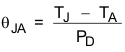
TJ = chip junction temperature
TA = ambient temperature
PD = device power dissipation
Factors that can greatly influence the measurement and calculation of θJA include:
- Whether or not the device is board mounted
- Trace size, composition, thickness, and geometry
- Orientation of the device (horizontal or vertical)
- Volume of the ambient air surrounding the device under test and airflow
- Whether other surfaces are in close proximity to the device being tested
The device power dissipation, PD, is a function of the charge rate and the voltage drop across the internal PowerFET. It can be calculated from the following equation when a battery pack is being charged:
PD = (VIN – VOUT) × IOUT
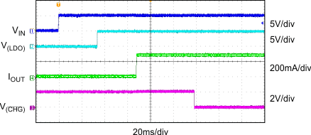
Due to the charge profile of LiFePO4 batteries the maximum power dissipation is typically seen at the beginning of the charge cycle when the battery voltage is at its lowest. See the charging profile, Figure 8. If the board thermal design is not adequate the programmed fast charge rate current may not be achieved under maximum input voltage and minimum battery voltage, as the thermal loop can be active, effectively reducing the charge current to avoid excessive IC junction temperature.
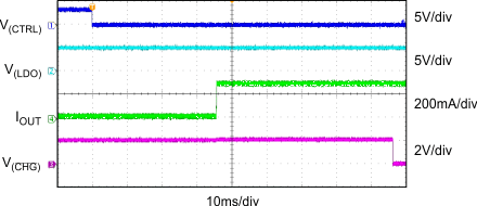
10.2.3 Application Curves
| V(CTRL) = 0 V | ||
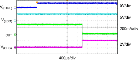
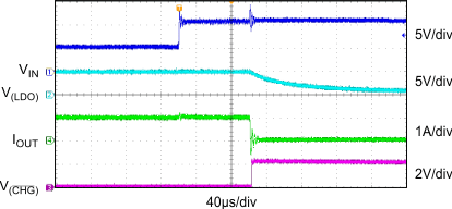
| VIN = 5 V to 12 V | ||