ZHCSCP1 July 2014
PRODUCTION DATA.
- 1 特性
- 2 应用
- 3 说明
- 4 应用信息
- 5 修订历史记录
- 6 Pin Configuration and Functions
- 7 Specifications
- 8 Detailed Description
- 9 Application and Implementation
- 10Power Supply Requirements
- 11Layout
- 12器件和文档支持
- 13机械封装和可订购信息
8 Detailed Description
8.1 Overview
The bq24311 is a highly integrated circuit designed to protect Li-ion batteries from charging circuit failures. The IC continuously monitors the input voltage, input current, and battery voltage. The input overvoltage protection immediately removes power from the charging circuit by turning off an internal switch. The input protection limits the system current at the user-programmable value, and if the overcurrent persists, switches the pass element OFF after a blanking period. Additionally, the IC also monitors its own die temperature and switches off if it becomes too hot.
8.2 Functional Block Diagram
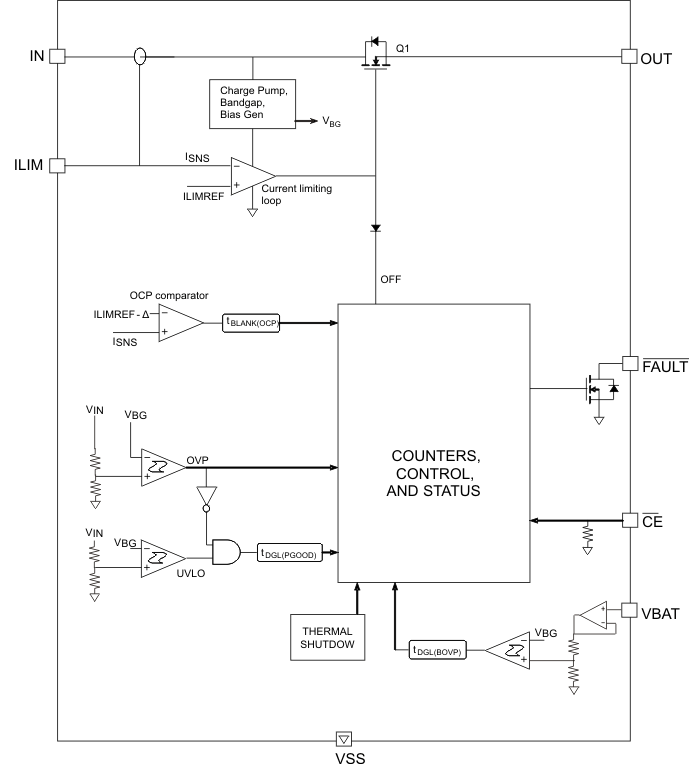 Figure 9. Simplified Block Diagram
8.3 Feature Description
8.3.1 Power Down
The device remains in power down mode when the voltage at the IN pin is below the undervoltage threshold VUVLO. The FET Q1 connected between IN and OUT pins is off, and the status output, FAULT, is set to Hi-Z.
8.3.2 Power-On Reset
The device resets when the voltage at the IN pin exceeds the UVLO threshold. All internal counters and other circuit blocks are reset. The IC then waits for duration tDGL(PGOOD) for the input voltage to stabilize. If, after tDGL(PGOOD), the input voltage and battery voltage are safe, FET Q1 is turned ON. The IC has a soft-start feature to control the inrush current which minimizes the ringing at input during power up, as shown in Figure 15 (ringing occurs because the parasitic inductance of the adapter cable and the input bypass capacitor form a resonant circuit). Because of the deglitch time at power-on, if the input voltage rises rapidly to beyond the OVP threshold, the device will not switch on at all, instead it will go into protection mode and indicate a fault on the FAULT pin, as shown in Figure 16.
8.4 Device Functional Modes
8.4.1 Operation
The device continuously monitors the input voltage, input current, and battery voltage as described in detail in the following sections.
8.4.1.1 Input Overvoltage Protection
If the input voltage rises above VOVP, the internal FET Q1 is turned off, removing power from the circuit. As shown in Figure 17, the response is rapid, with the FET turning off in less than a microsecond. The FAULT pin is driven low. When the input voltage returns below VOVP – VHYS-OVP (but is still above VUVLO), the FET Q1 is turned on again after a deglitch time of tON(OVP) to ensure that the input supply has stabilized. Figure 18 shows the recovery from input OVP.
8.4.1.2 Input Overcurrent Protection
If the load current tries to exceed the IOCP threshold, the device limits the current for a blanking period, tBLANK(OCP). If the load current returns to less than IOCP before tBLANK(OCP) times out, the device continues to operate. However, if the overcurrent situation persists for tBLANK(OCP), the FET Q1 is turned off for a duration of tREC(OCP), and the FAULT pin is driven low. The FET is then turned on again after tREC(OCP) and the current is monitored all over again. Each time an OCP fault occurs, an internal counter is incremented. If 15 OCP faults occur in one charge cycle, the FET is turned off permanently, as shown in Figure 19. The counter is cleared either by removing and re-applying input power, or by disabling and re-enabling the device with the CE pin. Figure 19 and Figure 20 show what happens in an overcurrent fault.
To prevent the input voltage from spiking up due to the inductance of the input cable, Q1 is turned off slowly, resulting in a “soft-stop”, as shown in Figure 22.
8.4.1.3 Battery Overvoltage Protection
The battery overvoltage threshold V(BOVP) is internally set to 4.35V. If the battery voltage exceeds the V(BOVP) threshold, the FET Q1 is turned off, and the FAULT pin is driven low. The FET is turned back on once the battery voltage drops to V(BOVP) – VHYS-BOVP (see Figure 22 and Figure 23). Each time a battery overvoltage fault occurs, an internal counter is incremented. If 15 such faults occur in one charge cycle, the FET is turned off permanently, as shown in Figure 23. The counter is cleared either by removing and re-applying input power, or by disabling and re-enabling the device with the CE pin. In the case of a battery overvoltage fault, Q1 is switched OFF gradually, resulting in a soft-stop (see Figure 22).
8.4.1.4 Thermal Protection
If the junction temperature of the device exceeds TJ(OFF), the FET Q1 is turned off, and the FAULT pin is driven low. The FET is turned back on when the junction temperature falls below TJ(OFF) – TJ(OFF-HYS).
8.4.1.5 Enable Function
The IC has an enable pin which can be used to enable or disable the device. When the CE pin is driven high, the internal FET is turned off. When the CE pin is low, the FET is turned on if other conditions are safe. The OCP counter and the Bat-OVP counter are both reset when the device is disabled and re-enabled. The CE pin has an internal pulldown resistor and can be left floating. Note that the FAULT pin functionality is also disabled when the CE pin is high.
8.4.1.6 Fault Indication
The FAULT pin is an active-low open-drain output. It is in a high-impedance state when operating conditions are safe, or when the device is disabled by setting CE high. With CE low, the FAULT pin goes low whenever any of these events occurs:
- Input overvoltage
- Input overcurrent
- Battery overvoltage
- IC Overtemperature
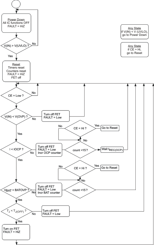 Figure 10. Flow Diagram