ZHCSCP1 July 2014
PRODUCTION DATA.
- 1 特性
- 2 应用
- 3 说明
- 4 应用信息
- 5 修订历史记录
- 6 Pin Configuration and Functions
- 7 Specifications
- 8 Detailed Description
- 9 Application and Implementation
- 10Power Supply Requirements
- 11Layout
- 12器件和文档支持
- 13机械封装和可订购信息
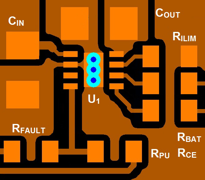
11 Layout
11.1 Layout Guidelines
- This device is a protection device, and is meant to protect down-stream circuitry from hazardous voltages. Potentially, high voltages may be applied to this IC. It has to be ensured that the edge-to-edge clearances of PCB traces satisfy the design rules for high voltages.
- The device uses SON packages with a PowerPAD™. For good thermal performance, the PowerPAD should be thermally coupled with the PCB ground plane. In most applications, this will require a copper pad directly under the IC. This copper pad should be connected to the ground plane with an array of thermal vias.
- CIN and COUT should be located close to the IC. Other components like RILIM and RBAT should also be located close to the IC.
11.2 Layout Example