ZHCSEZ6D April   2016  – January 2019

PRODUCTION DATA.  

  1. 特性
  2. 应用
  3. 说明
    1.     Device Images
      1.      简化原理图
  4. 修订历史记录
  5. Device Comparison
  6. Pin Configuration and Functions
    1.     Pin Functions
  7. Specifications
    1. 7.1 Absolute Maximum Ratings
    2. 7.2 ESD Ratings
    3. 7.3 Recommended Operating Conditions
    4. 7.4 Thermal Information
    5. 7.5 Electrical Characteristics
    6. 7.6 Timing Requirements
    7. 7.7 Typical Operational Characteristics (Protection Circuits Waveforms)
  8. Detailed Description
    1. 8.1 Overview
    2. 8.2 Functional Block Diagram
    3. 8.3 Feature Description
      1. 8.3.1 Power-Down or Undervoltage Lockout (UVLO)
      2. 8.3.2 Power-up
      3. 8.3.3 Sleep Mode
      4. 8.3.4 New Charge Cycle
      5. 8.3.5 Overvoltage-Protection (OVP) – Continuously Monitored
      6. 8.3.6 CHG Terminal Indication
    4. 8.4 Device Functional Modes
      1. 8.4.1  CHG LED Pull-up Source
      2. 8.4.2  IN-DPM (VIN-DPM or IN-DPM)
      3. 8.4.3  OUT
      4. 8.4.4  ISET
      5. 8.4.5  TS
      6. 8.4.6  Termination and Timer Disable Mode (TTDM) - TS Terminal High
      7. 8.4.7  Timers
      8. 8.4.8  Termination
      9. 8.4.9  Battery Detect Routine
      10. 8.4.10 Refresh Threshold
      11. 8.4.11 Starting a Charge on a Full Battery
  9. Application and Implementation
    1. 9.1 Application Information
    2. 9.2 Typical Application
      1. 9.2.1 Design Requirements
      2. 9.2.2 Detailed Design Procedure
        1. 9.2.2.1 Calculations
          1. 9.2.2.1.1 Program the Fast Charge Current, ISET:
          2. 9.2.2.1.2 Pre-Charge and Termination Current Thresholds, ITERM, and PRE-CHG
          3. 9.2.2.1.3 TS Function
          4. 9.2.2.1.4 CHG
        2. 9.2.2.2 Selecting In and Out Terminal Capacitors
      3. 9.2.3 Application Curves
  10. 10Power Supply Recommendations
  11. 11Layout
    1. 11.1 Layout Guidelines
    2. 11.2 Layout Example
    3. 11.3 Thermal Considerations
      1. 11.3.1 Leakage Current Effects on Battery Capacity
  12. 12器件和文档支持
    1. 12.1 接收文档更新通知
    2. 12.2 社区资源
    3. 12.3 商标
    4. 12.4 静电放电警告
    5. 12.5 术语表
  13. 13机械、封装和可订购信息

封装选项

机械数据 (封装 | 引脚)
散热焊盘机械数据 (封装 | 引脚)
订购信息

New Charge Cycle

A new charge cycle is started when a good power source is applied, performing a chip disable/enable (TS terminal), exiting Termination and Timer Disable Mode (TTDM), detecting a battery insertion or the OUT voltage dropping below the VRCH threshold. The CHG terminal is active low only during the first charge cycle, therefore exiting TTDM or a dropping below VRCH will not turn on the CHG terminal FET, if the CHG terminal is already high impedance.

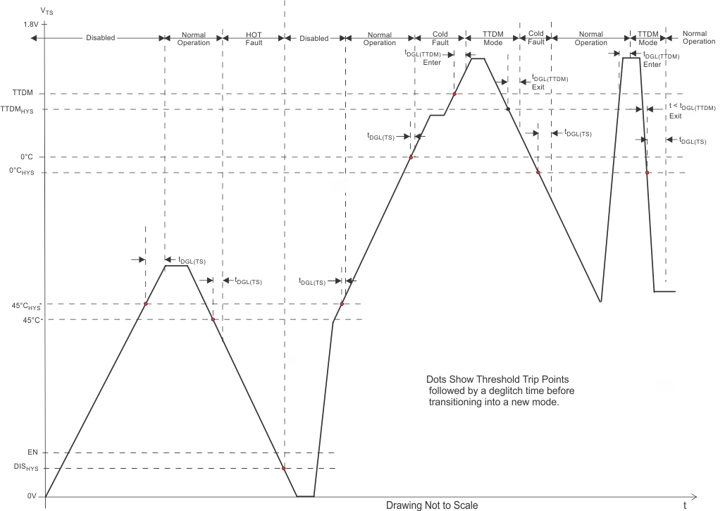
bq21040 batt_temp_slusce2.gifFigure 6. TS Battery Temperature Bias Threshold and Deglitch Timers
bq21040 power-up_flow_slusce2.gifFigure 7. bq21040 Power-Up Flow Diagram