ZHCS488K October 2011 – December 2018 AM3351 , AM3352 , AM3354 , AM3356 , AM3357 , AM3358 , AM3359
PRODUCTION DATA.
- 1器件概述
- 2修订历史记录
- 3Device Comparison
- 4Terminal Configuration and Functions
-
5Specifications
- 5.1 Absolute Maximum Ratings
- 5.2 ESD Ratings
- 5.3 Power-On Hours (POH)
- 5.4 Operating Performance Points (OPPs)
- 5.5 Recommended Operating Conditions
- 5.6 Power Consumption Summary
- 5.7 DC Electrical Characteristics
- 5.8 Thermal Resistance Characteristics for ZCE and ZCZ Packages
- 5.9 External Capacitors
- 5.10 Touch Screen Controller and Analog-to-Digital Subsystem Electrical Parameters
-
6Power and Clocking
- 6.1 Power Supplies
- 6.2
Clock Specifications
- 6.2.1 Input Clock Specifications
- 6.2.2 Input Clock Requirements
- 6.2.3 Output Clock Specifications
- 6.2.4 Output Clock Characteristics
-
7Peripheral Information and Timings
- 7.1 Parameter Information
- 7.2 Recommended Clock and Control Signal Transition Behavior
- 7.3 OPP50 Support
- 7.4 Controller Area Network (CAN)
- 7.5 DMTimer
- 7.6
Ethernet Media Access Controller (EMAC) and Switch
- 7.6.1
EMAC and Switch Electrical Data and Timing
- Table 7-7 EMAC and Switch Timing Conditions
- 7.6.1.1 EMAC/Switch MDIO Electrical Data and Timing
- 7.6.1.2
EMAC and Switch MII Electrical Data and Timing
- Table 7-11 Timing Requirements for GMII[x]_RXCLK - MII Mode
- Table 7-12 Timing Requirements for GMII[x]_TXCLK - MII Mode
- Table 7-13 Timing Requirements for GMII[x]_RXD[3:0], GMII[x]_RXDV, and GMII[x]_RXER - MII Mode
- Table 7-14 Switching Characteristics for GMII[x]_TXD[3:0], and GMII[x]_TXEN - MII Mode
- 7.6.1.3 EMAC and Switch RMII Electrical Data and Timing
- 7.6.1.4
EMAC and Switch RGMII Electrical Data and Timing
- Table 7-18 Timing Requirements for RGMII[x]_RCLK - RGMII Mode
- Table 7-19 Timing Requirements for RGMII[x]_RD[3:0], and RGMII[x]_RCTL - RGMII Mode
- Table 7-20 Switching Characteristics for RGMII[x]_TCLK - RGMII Mode
- Table 7-21 Switching Characteristics for RGMII[x]_TD[3:0], and RGMII[x]_TCTL - RGMII Mode
- 7.6.1
EMAC and Switch Electrical Data and Timing
- 7.7
External Memory Interfaces
- 7.7.1 General-Purpose Memory Controller (GPMC)
- 7.7.2
mDDR(LPDDR), DDR2, DDR3, DDR3L Memory Interface
- 7.7.2.1
mDDR (LPDDR) Routing Guidelines
- 7.7.2.1.1 Board Designs
- 7.7.2.1.2 LPDDR Interface
- 7.7.2.1.3 LPDDR CK and ADDR_CTRL Routing
- 7.7.2.2
DDR2 Routing Guidelines
- 7.7.2.2.1 Board Designs
- 7.7.2.2.2
DDR2 Interface
- 7.7.2.2.2.1 DDR2 Interface Schematic
- 7.7.2.2.2.2 Compatible JEDEC DDR2 Devices
- 7.7.2.2.2.3 PCB Stackup
- 7.7.2.2.2.4 Placement
- 7.7.2.2.2.5 DDR2 Keepout Region
- 7.7.2.2.2.6 Bulk Bypass Capacitors
- 7.7.2.2.2.7 High-Speed (HS) Bypass Capacitors
- 7.7.2.2.2.8 Net Classes
- 7.7.2.2.2.9 DDR2 Signal Termination
- 7.7.2.2.2.10 DDR_VREF Routing
- 7.7.2.2.3 DDR2 CK and ADDR_CTRL Routing
- 7.7.2.3
DDR3 and DDR3L Routing Guidelines
- 7.7.2.3.1 Board Designs
- 7.7.2.3.2 DDR3 Device Combinations
- 7.7.2.3.3
DDR3 Interface
- 7.7.2.3.3.1 DDR3 Interface Schematic
- 7.7.2.3.3.2 Compatible JEDEC DDR3 Devices
- 7.7.2.3.3.3 PCB Stackup
- 7.7.2.3.3.4 Placement
- 7.7.2.3.3.5 DDR3 Keepout Region
- 7.7.2.3.3.6 Bulk Bypass Capacitors
- 7.7.2.3.3.7 High-Speed Bypass Capacitors
- 7.7.2.3.3.8 Net Classes
- 7.7.2.3.3.9 DDR3 Signal Termination
- 7.7.2.3.3.10 DDR_VREF Routing
- 7.7.2.3.3.11 VTT
- 7.7.2.3.4 DDR3 CK and ADDR_CTRL Topologies and Routing Definition
- 7.7.2.3.5 Data Topologies and Routing Definition
- 7.7.2.3.6 Routing Specification
- 7.7.2.1
mDDR (LPDDR) Routing Guidelines
- 7.8 I2C
- 7.9 JTAG Electrical Data and Timing
- 7.10 LCD Controller (LCDC)
- 7.11 Multichannel Audio Serial Port (McASP)
- 7.12 Multichannel Serial Port Interface (McSPI)
- 7.13
Multimedia Card (MMC) Interface
- 7.13.1
MMC Electrical Data and Timing
- Table 7-89 MMC Timing Conditions
- Table 7-90 Timing Requirements for MMC[x]_CMD and MMC[x]_DAT[7:0]
- Table 7-91 Switching Characteristics for MMC[x]_CLK
- Table 7-92 Switching Characteristics for MMC[x]_CMD and MMC[x]_DAT[7:0]—Standard Mode
- Table 7-93 Switching Characteristics for MMC[x]_CMD and MMC[x]_DAT[7:0]—High-Speed Mode
- 7.13.1
MMC Electrical Data and Timing
- 7.14
Programmable Real-Time Unit Subsystem and Industrial Communication Subsystem (PRU-ICSS)
- 7.14.1 Programmable Real-Time Unit (PRU-ICSS PRU)
- 7.14.2
PRU-ICSS EtherCAT (PRU-ICSS ECAT)
- Table 7-100 PRU-ICSS ECAT Timing Conditions
- 7.14.2.1
PRU-ICSS ECAT Electrical Data and Timing
- Table 7-101 PRU-ICSS ECAT Timing Requirements – Input Validated With LATCH_IN
- Table 7-102 PRU-ICSS ECAT Timing Requirements – Input Validated With SYNCx
- Table 7-103 PRU-ICSS ECAT Timing Requirements – Input Validated With Start of Frame (SOF)
- Table 7-104 PRU-ICSS ECAT Timing Requirements - LATCHx_IN
- Table 7-105 PRU-ICSS ECAT Switching Requirements - Digital I/Os
- 7.14.3 PRU-ICSS MII_RT and Switch
- 7.14.4 PRU-ICSS Universal Asynchronous Receiver Transmitter (PRU-ICSS UART)
- 7.15 Universal Asynchronous Receiver Transmitter (UART)
- 8Device and Documentation Support
- 9Mechanical, Packaging, and Orderable Information
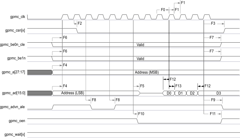
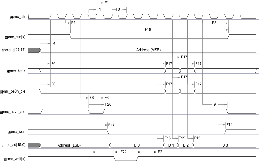
Table 7-24 GPMC and NOR Flash Switching Characteristics—Synchronous Mode(2)
| NO. | PARAMETER | OPP100 | OPP50 | UNIT | ||||
|---|---|---|---|---|---|---|---|---|
| MIN | MAX | MIN | MAX | |||||
| F0 | 1 / tc(clk) | Frequency(18), output clock gpmc_clk | 100 | 50 | MHz | |||
| F1 | tw(clkH) | Typical pulse duration, output clock gpmc_clk high | 0.5P(15) | 0.5P(15) | 0.5P(15) | 0.5P(15) | ns | |
| F1 | tw(clkL) | Typical pulse duration, output clock gpmc_clk low | 0.5P(15) | 0.5P(15) | 0.5P(15) | 0.5P(15) | ns | |
| tdc(clk) | Duty cycle error, output clock gpmc_clk | –500 | 500 | –500 | 500 | ps | ||
| tJ(clk) | Jitter standard deviation(19), output clock gpmc_clk | 33.33 | 33.33 | ps | ||||
| F2 | td(clkH-csnV) | Delay time, output clock gpmc_clk rising edge to output chip select gpmc_csn[x](14) transition | F(6) - 2.2 | F(6) + 4.5 | F(6) - 3.2 | F(6) + 9.5 | ns | |
| F3 | td(clkH-csnIV) | Delay time, output clock gpmc_clk rising edge to output chip select gpmc_csn[x](14) invalid | E(5) – 2.2 | E(5) + 4.5 | E(5) – 3.2 | E(5) + 9.5 | ns | |
| F4 | td(aV-clk) | Delay time, output address gpmc_a[27:1] valid to output clock gpmc_clk first edge | B(2) – 4.5 | B(2) + 2.3 | B(2) – 5.5 | B(2) + 12.3 | ns | |
| F5 | td(clkH-aIV) | Delay time, output clock gpmc_clk rising edge to output address gpmc_a[27:1] invalid | –2.3 | 4.5 | –3.3 | 14.5 | ns | |
| F6 | td(be[x]nV-clk) | Delay time, output lower byte enable and command latch enable gpmc_be0n_cle, output upper byte enable gpmc_be1n valid to output clock gpmc_clk first edge | B(2) – 1.9 | B(2) + 2.3 | B(2) – 2.9 | B(2) + 12.3 | ns | |
| F7 | td(clkH-be[x]nIV) | Delay time, output clock gpmc_clk rising edge to output lower byte enable and command latch enable gpmc_be0n_cle, output upper byte enable gpmc_be1n invalid(11) | D(4) – 2.3 | D(4) + 1.9 | D(4) – 3.3 | D(4) + 6.9 | ns | |
| F7 | td(clkL-be[x]nIV) | Delay time, gpmc_clk falling edge to gpmc_nbe0_cle, gpmc_nbe1 invalid(12) | D(4) – 2.3 | D(4) + 1.9 | D(4) – 3.3 | D(4) + 6.9 | ns | |
| F7 | td(clkL-be[x]nIV) | Delay time, gpmc_clk falling edge to gpmc_nbe0_cle, gpmc_nbe1 invalid(13) | D(4) – 2.3 | D(4) + 1.9 | D(4) – 3.3 | D(4) + 11.9 | ns | |
| F8 | td(clkH-advn) | Delay time, output clock gpmc_clk rising edge to output address valid and address latch enable gpmc_advn_ale transition | G(7) – 2.3 | G(7) + 4.5 | G(7) – 3.3 | G(7) + 9.5 | ns | |
| F9 | td(clkH-advnIV) | Delay time, output clock gpmc_clk rising edge to output address valid and address latch enable gpmc_advn_ale invalid | D(4) – 2.3 | D(4) + 3.5 | D(4) – 3.3 | D(4) + 9.5 | ns | |
| F10 | td(clkH-oen) | Delay time, output clock gpmc_clk rising edge to output enable gpmc_oen transition | H(8) – 2.3 | H(8) + 3.5 | H(8) – 3.3 | H(8) + 8.5 | ns | |
| F11 | td(clkH-oenIV) | Delay time, output clock gpmc_clk rising edge to output enable gpmc_oen invalid | H(8) – 2.3 | H(8) + 3.5 | H(8) – 3.3 | H(8) + 8.5 | ns | |
| F14 | td(clkH-wen) | Delay time, output clock gpmc_clk rising edge to output write enable gpmc_wen transition | I(9) – 2.3 | I(9) + 4.5 | I(9) – 3.3 | I(9) + 9.5 | ns | |
| F15 | td(clkH-do) | Delay time, output clock gpmc_clk rising edge to output data gpmc_ad[15:0] transition(11) | J(10) – 2.3 | J(10) + 1.9 | J(10) – 3.3 | J(10) + 6.9 | ns | |
| F15 | td(clkL-do) | Delay time, gpmc_clk falling edge to gpmc_ad[15:0] data bus transition(12) | J(10) – 2.3 | J(10) + 1.9 | J(10) – 3.3 | J(10) + 6.9 | ns | |
| F15 | td(clkL-do) | Delay time, gpmc_clk falling edge to gpmc_ad[15:0] data bus transition(13) | J(10) – 2.3 | J(10) + 1.9 | J(10) – 3.3 | J(10) + 11.9 | ns | |
| F17 | td(clkH-be[x]n) | Delay time, output clock gpmc_clk rising edge to output lower byte enable and command latch enable gpmc_be0n_cle transition(11) | J(10) – 2.3 | J(10) + 1.9 | J(10) – 3.3 | J(10) + 6.9 | ns | |
| F17 | td(clkL-be[x]n) | Delay time, gpmc_clk falling edge to gpmc_nbe0_cle, gpmc_nbe1 transition(12) | J(10) – 2.3 | J(10) + 1.9 | J(10) – 3.3 | J(10) + 6.9 | ns | |
| F17 | td(clkL-be[x]n) | Delay time, gpmc_clk falling edge to gpmc_nbe0_cle, gpmc_nbe1 transition(13) | J(10) – 2.3 | J(10) + 1.9 | J(10) – 3.3 | J(10) + 11.9 | ns | |
| F18 | tw(csnV) | Pulse duration, output chip select gpmc_csn[x](14) low | Read | A(1) | A(1) | ns | ||
| Write | A(1) | A(1) | ns | |||||
| F19 | tw(be[x]nV) | Pulse duration, output lower byte enable and command latch enable gpmc_be0n_cle, output upper byte enable gpmc_be1n low | Read | C(3) | C(3) | ns | ||
| Write | C(3) | C(3) | ns | |||||
| F20 | tw(advnV) | Pulse duration, output address valid and address latch enable gpmc_advn_ale low | Read | K(16) | K(16) | ns | ||
| Write | K(16) | K(16) | ns | |||||
- For single read: A = (CSRdOffTime – CSOnTime) × (TimeParaGranularity + 1) × GPMC_FCLK(17)
For burst read: A = (CSRdOffTime – CSOnTime + (n – 1) × PageBurstAccessTime) × (TimeParaGranularity + 1) × GPMC_FCLK(17)
For burst write: A = (CSWrOffTime – CSOnTime + (n – 1) × PageBurstAccessTime) × (TimeParaGranularity + 1) × GPMC_FCLK(17)
With n being the page burst access number. - B = ClkActivationTime × GPMC_FCLK(17)
- For single read: C = RdCycleTime × (TimeParaGranularity + 1) × GPMC_FCLK (17)
For burst read: C = (RdCycleTime + (n – 1) × PageBurstAccessTime) × (TimeParaGranularity + 1) × GPMC_FCLK(17)
For burst write: C = (WrCycleTime + (n – 1) × PageBurstAccessTime) × (TimeParaGranularity + 1) × GPMC_FCLK(17)
With n being the page burst access number. - For single read: D = (RdCycleTime – AccessTime) × (TimeParaGranularity + 1) × GPMC_FCLK(17)
For burst read: D = (RdCycleTime – AccessTime) × (TimeParaGranularity + 1) × GPMC_FCLK(17)
For burst write: D = (WrCycleTime – AccessTime) × (TimeParaGranularity + 1) × GPMC_FCLK(17) - For single read: E = (CSRdOffTime – AccessTime) × (TimeParaGranularity + 1) × GPMC_FCLK(17)
For burst read: E = (CSRdOffTime – AccessTime) × (TimeParaGranularity + 1) × GPMC_FCLK(17)
For burst write: E = (CSWrOffTime – AccessTime) × (TimeParaGranularity + 1) × GPMC_FCLK(17) - For csn falling edge (CS activated):
- Case GpmcFCLKDivider = 0:
- F = 0.5 × CSExtraDelay × GPMC_FCLK(17)
- Case GpmcFCLKDivider = 1:
- Case GpmcFCLKDivider = 2:
- F = 0.5 × CSExtraDelay × GPMC_FCLK(17) if ((CSOnTime – ClkActivationTime) is a multiple of 3)
- F = (1 + 0.5 × CSExtraDelay) × GPMC_FCLK(17) if ((CSOnTime – ClkActivationTime – 1) is a multiple of 3)
- F = (2 + 0.5 × CSExtraDelay) × GPMC_FCLK(17) if ((CSOnTime – ClkActivationTime – 2) is a multiple of 3)
- Case GpmcFCLKDivider = 0:
- For ADV falling edge (ADV activated):
- Case GpmcFCLKDivider = 0:
- G = 0.5 × ADVExtraDelay × GPMC_FCLK(17)
- Case GpmcFCLKDivider = 1:
- Case GpmcFCLKDivider = 2:
- G = 0.5 × ADVExtraDelay × GPMC_FCLK(17) if ((ADVOnTime – ClkActivationTime) is a multiple of 3)
- G = (1 + 0.5 × ADVExtraDelay) × GPMC_FCLK(17) if ((ADVOnTime – ClkActivationTime – 1) is a multiple of 3)
- G = (2 + 0.5 × ADVExtraDelay) × GPMC_FCLK(17) if ((ADVOnTime – ClkActivationTime – 2) is a multiple of 3)
For ADV rising edge (ADV deactivated) in Reading mode:- Case GpmcFCLKDivider = 0:
- G = 0.5 × ADVExtraDelay × GPMC_FCLK(17)
- Case GpmcFCLKDivider = 1:
- Case GpmcFCLKDivider = 2:
- G = 0.5 × ADVExtraDelay × GPMC_FCLK(17) if ((ADVRdOffTime – ClkActivationTime) is a multiple of 3)
- G = (1 + 0.5 × ADVExtraDelay) × GPMC_FCLK(17) if ((ADVRdOffTime – ClkActivationTime – 1) is a multiple of 3)
- G = (2 + 0.5 × ADVExtraDelay) × GPMC_FCLK(17) if ((ADVRdOffTime – ClkActivationTime – 2) is a multiple of 3)
For ADV rising edge (ADV deactivated) in Writing mode:- Case GpmcFCLKDivider = 0:
- G = 0.5 × ADVExtraDelay × GPMC_FCLK(17)
- Case GpmcFCLKDivider = 1:
- Case GpmcFCLKDivider = 2:
- G = 0.5 × ADVExtraDelay × GPMC_FCLK(17) if ((ADVWrOffTime – ClkActivationTime) is a multiple of 3)
- G = (1 + 0.5 × ADVExtraDelay) × GPMC_FCLK(17) if ((ADVWrOffTime – ClkActivationTime – 1) is a multiple of 3)
- G = (2 + 0.5 × ADVExtraDelay) × GPMC_FCLK(17) if ((ADVWrOffTime – ClkActivationTime – 2) is a multiple of 3)
- Case GpmcFCLKDivider = 0:
- For OE falling edge (OE activated) and I/O DIR rising edge (Data Bus input direction):
- Case GpmcFCLKDivider = 0:
- H = 0.5 × OEExtraDelay × GPMC_FCLK(17)
- Case GpmcFCLKDivider = 1:
- Case GpmcFCLKDivider = 2:
- H = 0.5 × OEExtraDelay × GPMC_FCLK(17) if ((OEOnTime – ClkActivationTime) is a multiple of 3)
- H = (1 + 0.5 × OEExtraDelay) × GPMC_FCLK(17) if ((OEOnTime – ClkActivationTime – 1) is a multiple of 3)
- H = (2 + 0.5 × OEExtraDelay) × GPMC_FCLK(17) if ((OEOnTime – ClkActivationTime – 2) is a multiple of 3)
For OE rising edge (OE deactivated):- Case GpmcFCLKDivider = 0:
- H = 0.5 × OEExtraDelay × GPMC_FCLK(17)
- Case GpmcFCLKDivider = 1:
- Case GpmcFCLKDivider = 2:
- H = 0.5 × OEExtraDelay × GPMC_FCLK(17) if ((OEOffTime – ClkActivationTime) is a multiple of 3)
- H = (1 + 0.5 × OEExtraDelay) × GPMC_FCLK(17) if ((OEOffTime – ClkActivationTime – 1) is a multiple of 3)
- H = (2 + 0.5 × OEExtraDelay) × GPMC_FCLK(17) if ((OEOffTime – ClkActivationTime – 2) is a multiple of 3)
- Case GpmcFCLKDivider = 0:
- For WE falling edge (WE activated):
- Case GpmcFCLKDivider = 0:
- I = 0.5 × WEExtraDelay × GPMC_FCLK(17)
- Case GpmcFCLKDivider = 1:
- Case GpmcFCLKDivider = 2:
- I = 0.5 × WEExtraDelay × GPMC_FCLK(17) if ((WEOnTime – ClkActivationTime) is a multiple of 3)
- I = (1 + 0.5 × WEExtraDelay) × GPMC_FCLK(17) if ((WEOnTime – ClkActivationTime – 1) is a multiple of 3)
- I = (2 + 0.5 × WEExtraDelay) × GPMC_FCLK(17) if ((WEOnTime – ClkActivationTime – 2) is a multiple of 3)
For WE rising edge (WE deactivated):- Case GpmcFCLKDivider = 0:
- I = 0.5 × WEExtraDelay × GPMC_FCLK (17)
- Case GpmcFCLKDivider = 1:
- Case GpmcFCLKDivider = 2:
- I = 0.5 × WEExtraDelay × GPMC_FCLK(17) if ((WEOffTime – ClkActivationTime) is a multiple of 3)
- I = (1 + 0.5 × WEExtraDelay) × GPMC_FCLK(17) if ((WEOffTime – ClkActivationTime – 1) is a multiple of 3)
- I = (2 + 0.5 × WEExtraDelay) × GPMC_FCLK(17) if ((WEOffTime – ClkActivationTime – 2) is a multiple of 3)
- Case GpmcFCLKDivider = 0:
- J = GPMC_FCLK(17)
- First transfer only for CLK DIV 1 mode.
- Half cycle; for all data after initial transfer for CLK DIV 1 mode.
- Half cycle of GPMC_CLK_OUT; for all data for modes other than CLK DIV 1 mode. GPMC_CLK_OUT divide down from GPMC_FCLK.
- In gpmc_csn[x], x is equal to 0, 1, 2, 3, 4, or 5. In gpmc_wait[x], x is equal to 0 or 1.
- P = gpmc_clk period in ns
- For read: K = (ADVRdOffTime – ADVOnTime) × (TimeParaGranularity + 1) × GPMC_FCLK(17)
For write: K = (ADVWrOffTime – ADVOnTime) × (TimeParaGranularity + 1) × GPMC_FCLK(17) - GPMC_FCLK is general-purpose memory controller internal functional clock period in ns.
- Related to the gpmc_clk output clock maximum and minimum frequencies programmable in the GPMC module by setting the GPMC_CONFIG1_CSx configuration register bit field GpmcFCLKDivider.
- The jitter probability density can be approximated by a Gaussian function.
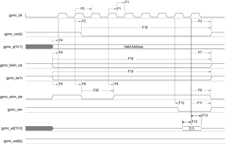
A. In gpmc_csn[x], x is equal to 0, 1, 2, 3, 4, or 5.
B. In gpmc_wait[x], x is equal to 0 or 1.
Figure 7-17 GPMC and NOR Flash—Synchronous Single Read—(GpmcFCLKDivider = 0)AB 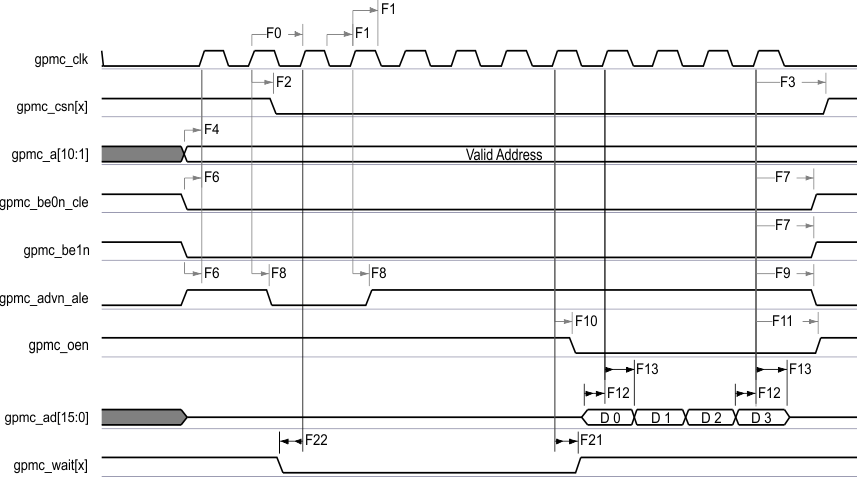
A. In gpmc_csn[x], x is equal to 0, 1, 2, 3, 4, or 5.
B. In gpmc_wait[x], x is equal to 0 or 1.
Figure 7-18 GPMC and NOR Flash—Synchronous Burst Read—4x16-Bit (GpmcFCLKDivider = 0)AB 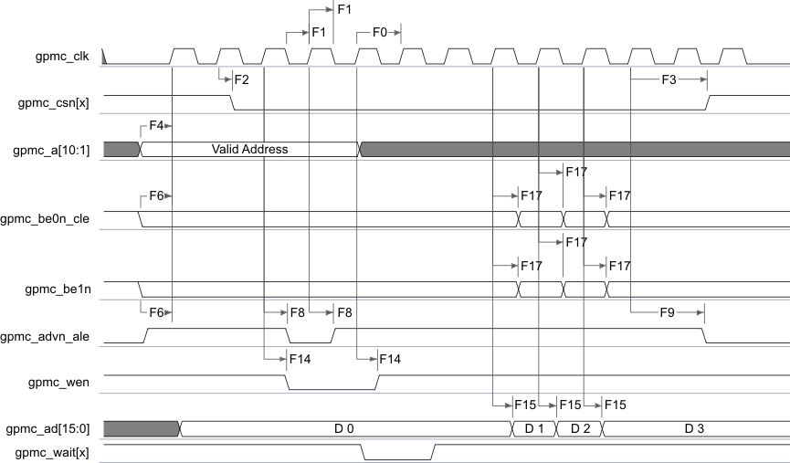
A. In gpmc_csn[x], x is equal to 0, 1, 2, 3, 4, or 5.
B. In gpmc_wait[x], x is equal to 0 or 1.
Figure 7-19 GPMC and NOR Flash—Synchronous Burst Write—(GpmcFCLKDivider > 0)AB 