ZHCSDN3B February 2015 – May 2015 ALM2402-Q1
PRODUCTION DATA.
- 1 特性
- 2 应用
- 3 说明
- 4 简化电路原理图
- 5 修订历史记录
- 6 Pin Configuration and Functions
- 7 Specifications
- 8 Detailed Description
- 9 Applications and Implementation
- 10Power Supply Recommendations
- 11Layout
- 12器件和文档支持
- 13机械、封装和可订购信息
封装选项
机械数据 (封装 | 引脚)
散热焊盘机械数据 (封装 | 引脚)
- PWP|14
订购信息
9 Applications and Implementation
NOTE
Information in the following applications sections is not part of the TI component specification, and TI does not warrant its accuracy or completeness. TI’s customers are responsible for determining suitability of components for their purposes. Customers should validate and test their design implementation to confirm system functionality.
9.1 Application Information
ALM2402Q1 is a dual power opamp with performance and protection features that are optimal for many applications. As it is an opamp, there are many general design consideration that must taken into account. Below will describe what to consider for most closed loop applications and gives a specific example of ALM2402Q1 being used in a motor drive application.
9.1.1 Capacitive Load and Stability
The ALM2402Q1 device is designed to be used in applications where driving a capacitive load is required. As with all op-amps, specific instances can occur where the ALM2402Q1 device can become unstable. The particular op-amp circuit configuration, layout, gain, and output loading are some of the factors to consider when establishing whether or not an amplifier is stable in operation. An op-amp in the unity-gain (1 V/V) buffer configuration that drives a capacitive load exhibits a greater tendency to be unstable than an amplifier operated at a higher noise gain. The capacitive load, in conjunction with the op-amp output resistance, creates a pole within the feedback loop that degrades the phase margin. The degradation of the phase margin increases as the capacitive loading increases. When operating in the unity-gain configuration, the ALM2402Q1 device remains stable with a pure capacitive load up to approximately 3µF. The equivalent series resistance (ESR) of some very large capacitors (CL greater than 1 μF) is sufficient to alter the phase characteristics in the feedback loop such that the amplifier remains stable. Increasing the amplifier closed-loop gain allows the amplifier to drive increasingly larger capacitance. This increased capability is evident when observing the overshoot response of the amplifier at higher voltage gains.
One technique for increasing the capacitive load drive capability of the amplifier operating in a unity-gain configuration is to insert a small resistor, typically 100mΩ to 10Ω, in series with the output (RS), as shown in Figure 25. This resistor significantly reduces the overshoot and ringing associated with large capacitive loads.
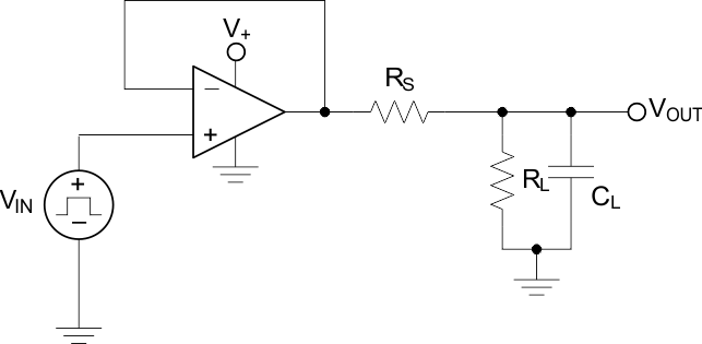 Figure 25. Capacitive Load Drive
Below are application curves displaying the step response of the above configuration with CL = 2.2 µF, RL = 10 MΩ and RL = 100 Ω. Displaying the ALM2402Q1's good stability performance with big capacitive loads.
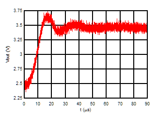 Figure 26. Output Pulse Response (CL = 2.2 µF and RL = 10 MΩ)
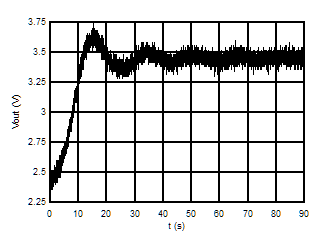 Figure 27. Output Pulse Response (CL = 2.2 µF and RL = 100 Ω)
9.2 Typical Application
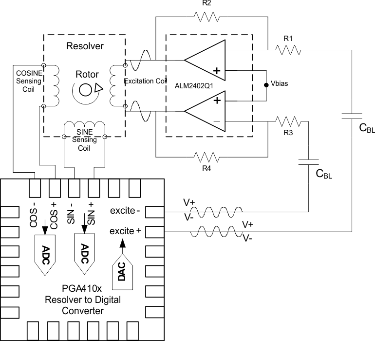 Figure 28. ALM2402Q1 in Resolver Application
High power AC and BLDC motor drive applications need angular and position feedback in order to efficiently and accurately drive the motor. Position feedback can be achieved by using optical encoders, hall sensors or resolvers. Resolvers are the go to choice when environmental or longevity requirements are challenging and extensive.
A resolver acts like a transformer with one primary coil and two secondary coils. The primary coil, or excitation coil, is located on the rotor of the resolver. As the rotor of the resolver spins, the excitation coil induces a current into the sine and cosine sensing coils. These coils are oriented 90 degrees from one another and produce a vector position read by the resolver to digital converter chip.
Resolver excitation coils can have a very low DC resistance (<100 Ω), causing a need of to sink and source up to 200 mA from the excitation driver. The ALM2402Q1 can source and sink this current while providing current limiting and thermal shutdown protection. Incorporating these protections in a resolver design can increase the life of the end product.
The fundamental design steps and ALM2402Q1 benefits shown in this application example can be applied to other inductive load applications like DC and servo motors. For more information on other applications that ALM2402Q1 offers a solution to please see (SLVA696), available for download from www.ti.com.
9.2.1 Design Requirements
For this design example, use the parameters listed in Table 2 as the input parameters.
Table 2. Design Parameters
| DESIGN PARAMETER | EXAMPLE VALUE |
|---|---|
| Ambient Temperature Range | -40°C to 125°C |
| Available Supply Voltages | 12 V, 5 V, 3.3 V |
| EMC Capacitance (CL) | 100 nF |
| Excitation Input Voltage Range | 2 Vrms - 7 Vrms |
| Excitation Frequency | 10 kHz |
9.2.2 Detailed Design Procedure
When using ALM2402Q1 in a resolver application, determine:
- Resolver Excitation Input Impedance or Resistance and Inductance: ZO= 50 + j188; (R = 50 Ω and L = 3 mH)
- Resolver Transformation Ration (VEXC/VSINCOS): 0.5 V/V at 10 kHz
- Package and θJA : DRR, 39.2°C/W
- Opamp Maximum Junction Temperature: 150ºC
- Opamp Bandwidth: 600 kHz
9.2.2.1 Resolver Excitation Input (Opamp Output)
Like a transformer, a resolver needs an alternating current input to function properly. The resolver takes this alternating current from the primary coil (excitation input) and creates a multiple of it on the secondary sides (SIN, COS ports). When determining how to generate this alternating current it is important to understand an opamp's ability or limitations. For the excitation input, the resolver input impedance, stability RMS voltage and desired frequency must be taken in to account:
9.2.2.1.1 Excitation Voltage
For this example, the resolver impedance is specified between 2Vrms and 7Vrms up 20kHz maximum frequency. Since, the resolver attenuation is ~0.5V/V and most data acquisition microelectronics run off of 5V supply voltages. An excitation input of 6Vpp (or 2.12Vrms) will be chosen to give the output readout circuitry enough headroom to measure the secondary side outputs (~3Vpp).
The excitation coil can be driven by a single-ended opamp output with the other side of the coil grounded or differentially as shown in Figure 28. Differential drive offers higher peak to peak voltage (double) on to the excitation coil, while not using up as much output voltage headroom from the opamp. Leading to lower distortion on the output signal.
Another consideration for excitation is opamp power dissipation. As described in Power Dissipation and Thermal Reliability, power dissipation from the opamp can be lowered by driving the output peak voltages close to the supply and ground voltages. With ALM2402Q1's very low VOH/VOL, this can be easily accomplished. Please see Figure 1 for VOH/VOL values with respect to output current and Output Stage for further description of the rail-rail output stage.
9.2.2.1.2 Excitation Frequency
The excitation frequency is chosen based on the desired secondary side output signal resolution. As shown in Figure 34, the excitation signal is similar to a sampling pulse in ADCs, with the real information being in the envelope created by the rotor. With a GBW of 600kHz, ALM2402Q1 has more than enough open loop gain at 10kHz to create negligible closed loop gain error.
Along with GBW, ALM2402Q1 has optimal THD and SR performance (see Typical Characteristics) to achieve 6Vpp (or 3Vpp from each opamp). The signal integrity can also be observed in the Typical Characteristics section.
9.2.2.1.3 Excitation Impedance
Knowledge of the primary side impedance is very important when chosing an opamp for this application. As shown below in Figure 29, the excitation coil looks like an inductance in series with a resistance. Many time these values aren't given and must by calculated from the cartesian or polar form, as it is given as a function of frequency or phase angle. This calculation is a trivial task.
Once the coil resistance is determined, the maximum or peak-peak current needed from ALM2402Q1 can be determined by below:

In this example the peak-peak output current equates to ~120mA. Each opamp will handle the peak current, with one sinking max and the other sourcing. Knowledge of the opamp current is very important when determining ALM2402Q1's power dissipation. Which is discussed in the Power Dissipation and Thermal Reliability section.
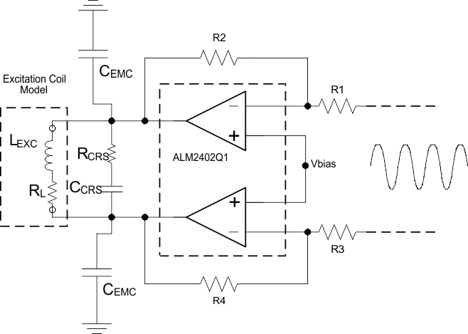 Figure 29. Excitation Coil Implementation
The primary side of a resolver is inductive, but that typically is not all the opamps driving the coils see. As shown in , many times designers will add a resistor in series with a capacitor to illiminate crossover distortion. Which happens due to the biasing of BJTs in the discrete implementation. With ALM2402Q1's rail-rail output, this is rarely needed. This can be seen in the waveforms shown in the section.
It is also common practice to add EMC capacitors to the opamp outputs to help shield other devices on the PCB from the radiation created by the motor and resolver. When choosing CEMC, it ismportant to take the opamp's stability in to account. With ALM2402Q1 having bery good phase margin at and above 200nF, no stability issues will be present for many typical CEMC values.
9.2.2.2 Resolver Output
As mentioned in the Excitation Frequency section, the excitation signal is similar to a sampling pulse in ADCs, with the real information being in the envelope created by the rotor. The equations below show the behavior of the sin and cos outputs. Whereby the excitation signal is attenuated and enveloped by the voltage created from the electromagnetic response of the rotating rotor. The resolver analog output to digital converter will filter out the excitation signal and process the sine and cosine angles produced by the rotor. Hince, signal intergity or the sine and cosine envelope is most important in resolver design and some trade-offs in signal integrity of the excitation signal can be made for cost or convenience. Many times users can use a square wave or sawtooth signal to accomplish excitation, as opposed to a sine wave.


9.2.2.3 Power Dissipation and Thermal Reliability
Very critical aspects to many industrial and automotive applications are operating temperature and power dissipation. Resolvers are typically chosen over other position feedback techniques due to their sustainability and accuracy in harsh conditions and very high temperatures.
Along with the resolver, the electronics used in this system must be able to withstand these conditions. ALM2402Q1 is Q100 qualified and is able to operate at temperatures up to 125°C. In order to insure that this device can withstand these temperatures, the internal power dissipation must be determined.
The total power dissipation from ALM2402Q1 in this application is the sum of the power from the input supply and output supplies.

As shown in the equation below. PSS is a function of the internal supply and operating current of both opamps (ICC). With this opamp being CMOS, the ICC will not increase proportionally to the load like a BJT based design. It will stay close to the average value listed in Electrical Characteristics.


As shown inFigure 30, the load current will flow out of one opamp, through the load and in to the other. Each opamp shares the same load at 180° phase difference. The PMOS and NMOS output transistors are resistive when driven near supply and ground. Operating the output voltage at a high percentage of the supply voltage will greatly limit the chip power dissipation. The Typical Characteristics section gives more information on the expected voltage drop, that can be used to determine the limits of VOUT.
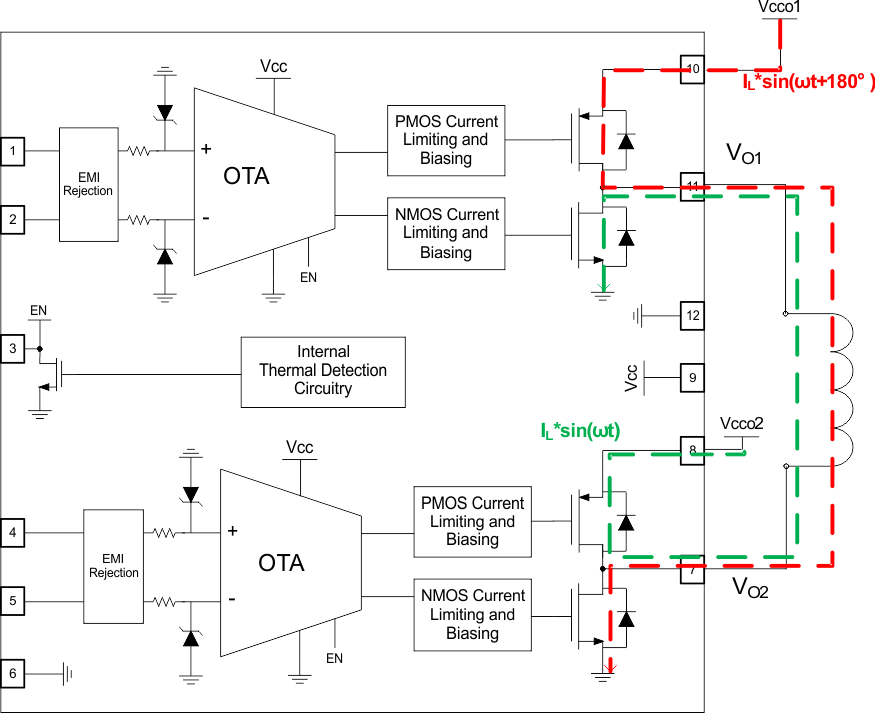 Figure 30. ALM2402Q1 Current Flow
After the total power dissipation is determined, the junction temperature at the worst expected ampient temperature case must be determined. This can be determined by Equation 9 below or from Figure 31.


For this example, the maximum junction temperature equates to ~144ºC which is in the safe operating region, below the maximum junction temperature of 150°C. It is required to limit ALM2402Q1's die junction temperature to less than 150°C. Please see Absolute Maximum Ratings table for further detail.
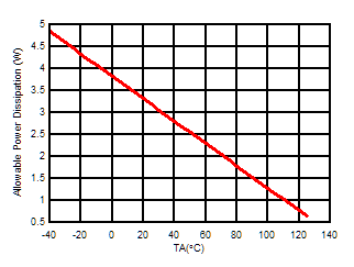
9.2.2.3.1 Improving Package Thermal Performance
θJA value depends on the PC board layout. An external heat sink and/or a cooling mechanism, like a cold air fan, can help reduce θJA and thus improve device thermal capabilities. Refer to TI’s design support web page at www.ti.com/thermal for a general guidance on improving device thermal performance.
9.2.3 Application Curves
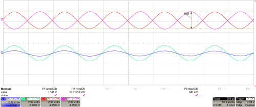
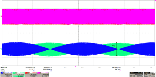
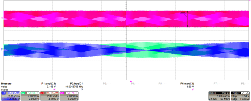
Below is test data with ALM2402Q1 exciting TE Connectivity (V23401-D1001-B102) Hollow Shaft Resolver.
Table 3. Waveform Legend
| Waveform Color | Description |
|---|---|
| Green | SINE output |
| Blue | COSINE output |
| Red | Excitation positive terminal inputs (referenced to ground) |
| Purple | Excitation negative terminal inputs (referenced to ground) |
