ZHCSDN3B February 2015 – May 2015 ALM2402-Q1
PRODUCTION DATA.
- 1 特性
- 2 应用
- 3 说明
- 4 简化电路原理图
- 5 修订历史记录
- 6 Pin Configuration and Functions
- 7 Specifications
- 8 Detailed Description
- 9 Applications and Implementation
- 10Power Supply Recommendations
- 11Layout
- 12器件和文档支持
- 13机械、封装和可订购信息
封装选项
机械数据 (封装 | 引脚)
散热焊盘机械数据 (封装 | 引脚)
- PWP|14
订购信息
8 Detailed Description
8.1 Overview
ALM2402Q1 is a dual power opamp with features and performance that make it preferable in many applications. Its high voltage tolerance, low offset and drift make it optimal in sensing applications. While its current limiting and over temperature detection make it very robust in applications that drive analog signal off of the PCB on to wires that are susceptible to faults from the outside world.
This device is optimal for applications that require high amounts of power. Its rail to rail output, enabled by the low Rdson PMOS and NMOS transistors keep the power dissipation low. The small 3mm x 3mm DRR package with its thermal pad and low θJA also allows users to deliver high currents to loads.
Other key features this device offers is its separate output driver supply (for external high-side current limit adjustability), wide stability range (with good phase margin up to 1uF) and shutdown capability (for applications that need low Icc).
8.2 Functional Block Diagram
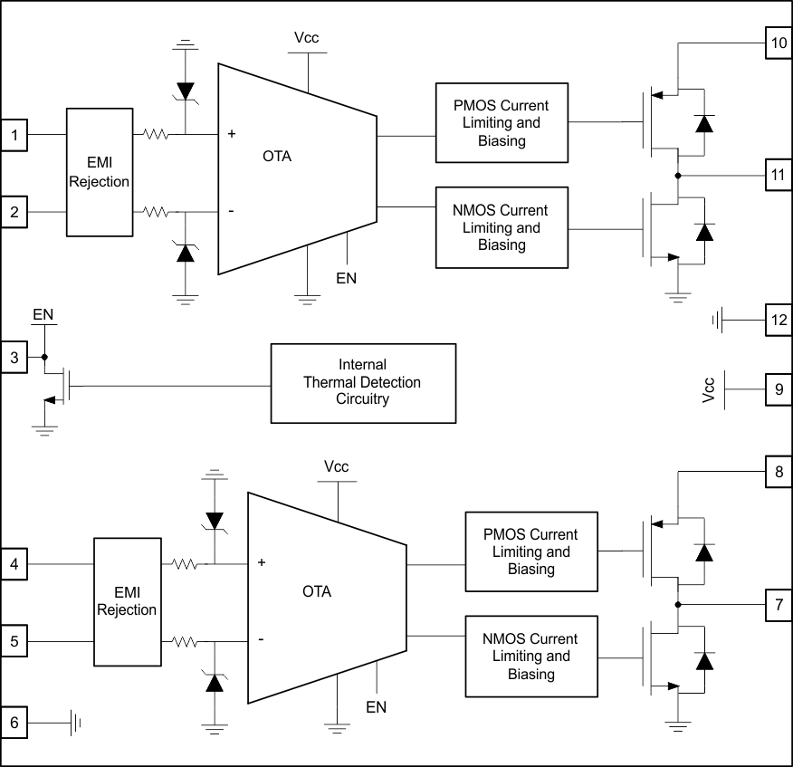
 Figure 23. Functional Block Diagram
8.3 Feature Description
8.3.1 OTF/SH_DN
The OTF/SH_DN pin is a bidirectional pin that will allow the user to put both opamps in to a low Iq state (<500µA) when forced low or below VIL_OTF. Due to this pin being bidirectional and it's Enable/Disable functionality, it must be pulled high or above VIH_OTF through a pullup resistor in order for the opamp to function properly or within the specs guaranteed in Electrical Characteristics.
When the junction temperature of ALM2402Q1 crosses the limits specified in Electrical Characteristics, the OTF/SH_DN pin will go low to alert the application that the both output have turned off due to an over temperature event. Also, the OTF pin will go low if VCC_O1 and VCC_O2 are 0 V.
When OTF/SH_DN is pulled low and the opamps are shutdown, the opamps will be in open-loop even when there is negative feedback applied. This is due to the loss of open loop gain in the opamps when the biasing is disabled. Please see Open Loop and Closed Loop for more detail on open and close loop considerations.
8.3.2 Supply Voltage
ALM2402Q1 uses three power rails. VCC powers the opamp signal path (OTA) and protection circuitry and VCC_O1 and VCC_O2 power the output high side driver.. Each supply can operate at separate voltages levels (higher or lower). The min and max values listed in Electrical Characteristics table are voltages that will enable ALM2402Q1 to properly function at or near the specification listed in Electrical Characteristics table. The specification listed in this table are guaranteed for 5 V and 12 V.
8.3.3 Current Limit and Short Circuit Protection
Each opamp in ALM2402Q1 has seperate internal current limiting for the PMOS (high-side) and NMOS (low-side) output transistors. If the output is shorted to ground then the PMOS (high-side) current limit is activated and will limit the current to 750mA nominally (see Electrical Characteristics) or to values shown in Figure 6 over temperature. If the output is shorted to supply then the NMOS (low-side) current limit is activated and will limit the current to 550mA nominally (see Electrical Characteristics) or to values shown in Figure 5 over temperature. The current limit value decreases with increasing temperature due to the temperature coefficient of a base-emitter junction voltage. Similarly, the current limit value increases at low temperatures.
A programmable current limit for short to ground scenarios can be achieved by adding resistance between VCC_O(X) and the supply (or battery).
When current is limited, the safe limits for the die temperature (see Recommended Operating Conditions and Absolute Maximum Ratings) must be taken in to account. With too much power dissipation, the die temperature can surpass the thermal shutdown limits and the opamp will shutdown and reactivate once the die has fallen below thermal limits. However, it is not recommended to continuously operate the device in thermal hysteresis for long periods of time (see Absolute Maximum Ratings).
8.3.4 Input Common Mode Range and Overvoltage Clamps
ALM2402Q1's input common mode range is between 0.2V and VCC-1.2V (see Electrical Characteristics). Staying withing this range will allow the opamps to perform and operate within the specification listed in Electrical Characteristics. Operating beyond these limits can cause distortion and non-linearities.
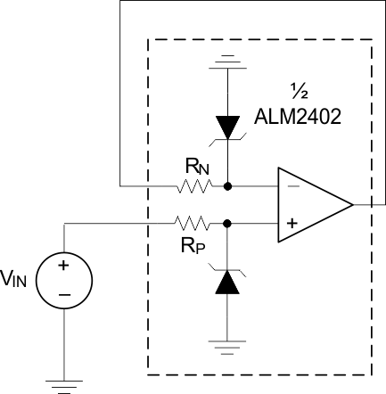
In order for the inputs to tolerate high voltages in the event of a short to supply, zener diodes have been added (see Figure 24). The current into this zener is limited via internal resistors. When operating near or above the zener voltage (7 V), the additional voltage gain error caused by the mismatch in internal resistors must be taken in to account. In unity gain, the opamp will force both gate voltages to be equal to the zener voltage on the positive input pin and ideally both zeners will sink the same amount of current and force the output voltage to be equal to Vin. In reality, RN and RP and VZ between both zener diodes do not perfectly match and have some % difference between their values. This leads to the output being Vo=Vin*(ΔR + ΔVZ) .
 Figure 24. Schematic Including Input Clamps
8.3.5 Thermal Shutdwon
If the die temperature exceeds safe limits, all outputs will be disabled, and the OTF/SH_DN pin will be driven low. Once the die temperature has fallen to a safe level, operation will automatically resume. The OTF/SH_DN pin will be released after operation has resumed.
When operating the die at a high temperature, the opamp will toggle on and off between the thermal shutdown hysteresis. In this event the safe limits for the die temperature (see Recommended Operating Conditions and Thermal Information) must be taken in to account. It is not recommended to continuously operate the device in thermal hysteresis for long periods of time (see Recommended Operating Conditions).
8.3.6 Output Stage
Designed as a high voltage, high current operational amplifier, the ALM2402Q1 device delivers a robust output drive capability. A class AB output stage with common-source transistors is used to achieve full rail-to-rail output swing capability. For resistive loads up to 10 kΩ, the output swings typically to within 5 mV of either supply rail regardless of the power-supply voltage applied. Different load conditions change the ability of the amplifier to swing close to the rails; refer to the graphs in Typical Characteristics section.
Each output transistor has internal reverse diodes between drain and source that will conduct if the output is forced higher than the supply or lower than ground (reverse current flow). Users may choose to use these as flyback protection in inductive load driving applications. Figure 7 show I-V characteristics of both diodes. It is recommended to limit the use of these diodes to pulsed operation to minimize junction temperature overheating due to (VF*IF). Internal current limiting circuitry will not operate when current is flown in the reverse direction and the reverse diodes are active.
8.3.7 EMI Susceptibility and Input Filtering
Op-amps vary with regard to the susceptibility of the device to electromagnetic interference (EMI). If conducted EMI enters the op-amp, the dc offset observed at the amplifier output may shift from the nominal value while EMI is present. This shift is a result of signal rectification associated with the internal semiconductor junctions. While all op-amp pin functions can be affected by EMI, the signal input pins are likely to be the most susceptible. The ALM2402Q1 device incorporates an internal input low-pass filter that reduces the amplifiers response to EMI. Both common-mode and differential mode filtering are provided by this filter.
Texas Instruments has developed the ability to accurately measure and quantify the immunity of an operational amplifier over a broad frequency spectrum extending from 10 MHz to 990 MHz. The EMI rejection ratio (EMIRR) metric allows op-amps to be directly compared by the EMI immunity. Figure 22 shows the results of this testing on the ALM2402Q1 device. Detailed information can also be found in the application report, EMI Rejection Ratio of Operational Amplifiers (SBOA128), available for download from www.ti.com
8.4 Device Functional Modes
8.4.1 Open Loop and Closed Loop
Due to its very high open loop DC gain, the ALM2402Q1 will function as a comparator in open loop for most applications. As noted in Electrical Characteristics table, the majority of electrical characteristics are verified in negative feedback, closed loop configurations. Certain DC electrical characteristics, like offset, may have a higher drift across temperature and lifetime when continuously operated in open loop over the lifetime of the device.
8.4.2 Shutdown
When the OTF/SH_DN pin is left floating or is grounded, the opamp will shutdown to a low Iq state and will not operate. The opamp outputs will go to a high impedance state. Please see OTF/SH_DN for more detailed information on OTF/SH_DN pin.
Table 1. Shutdown Truth Table
| Logic State | Opamp State | |
|---|---|---|
| OTF/SH_DN | High ( > VIH_OTF see Recommended Operating Conditions) | Operating |
| Low ( < VIL_OTF see Recommended Operating Conditions) | Shutdown (low Iq state) |