ZHCSBO2H December   2012  – July 2014 AFE4400

PRODUCTION DATA.  

  1. 特性
  2. 应用
  3. 说明
  4. 修订历史记录
  5. Device Family Options
  6. Pin Configuration and Functions
  7. Specifications
    1. 7.1 Absolute Maximum Ratings
    2. 7.2 Handling Ratings
    3. 7.3 Recommended Operating Conditions
    4. 7.4 Thermal Information
    5. 7.5 Electrical Characteristics
    6. 7.6 Timing Requirements
    7. 7.7 Timing Requirements: Supply Ramp and Power-Down
    8. 7.8 Typical Characteristics
  8. Detailed Description
    1. 8.1 Overview
    2. 8.2 Functional Block Diagram
    3. 8.3 Feature Description
      1. 8.3.1 Receiver Channel
        1. 8.3.1.1 Receiver Front-End
        2. 8.3.1.2 Ambient Cancellation Scheme and Second Stage Gain Block
        3. 8.3.1.3 Receiver Control Signals
        4. 8.3.1.4 Receiver Timing
      2. 8.3.2 Clocking and Timing Signal Generation
      3. 8.3.3 Timer Module
        1. 8.3.3.1 Using the Timer Module
      4. 8.3.4 Receiver Subsystem Power Path
      5. 8.3.5 Transmit Section
        1. 8.3.5.1 Transmitter Power Path
        2. 8.3.5.2 LED Power Reduction During Periods of Inactivity
    4. 8.4 Device Functional Modes
      1. 8.4.1 ADC Operation and Averaging Module
        1. 8.4.1.1 Operation
      2. 8.4.2 Diagnostics
        1. 8.4.2.1 Photodiode-Side Fault Detection
        2. 8.4.2.2 Transmitter-Side Fault Detection
        3. 8.4.2.3 Diagnostics Module
    5. 8.5 Programming
      1. 8.5.1 Serial Programming Interface
      2. 8.5.2 Reading and Writing Data
        1. 8.5.2.1 Writing Data
        2. 8.5.2.2 Reading Data
        3. 8.5.2.3 Multiple Data Reads and Writes
        4. 8.5.2.4 Register Initialization
        5. 8.5.2.5 AFE SPI Interface Design Considerations
    6. 8.6 Register Maps
      1. 8.6.1 AFE Register Map
      2. 8.6.2 AFE Register Description
  9. Applications and Implementation
    1. 9.1 Application Information
    2. 9.2 Typical Application
      1. 9.2.1 Design Requirements
      2. 9.2.2 Detailed Design Procedure
      3. 9.2.3 Application Curve
  10. 10Power Supply Recommendations
  11. 11Layout
    1. 11.1 Layout Guidelines
    2. 11.2 Layout Example
  12. 12器件和文档支持
    1. 12.1 Trademarks
    2. 12.2 Electrostatic Discharge Caution
    3. 12.3 术语表
  13. 13机械封装和可订购信息

封装选项

机械数据 (封装 | 引脚)
散热焊盘机械数据 (封装 | 引脚)
订购信息

11 Layout

11.1 Layout Guidelines

Some key layout guidelines are mentioned below:

  1. TXP, TXN are fast-switching lines and should be routed away from sensitive reference lines as well as from the INP, INN inputs.
  2. If the INP, INN lines are required to be routed over a long trace, TI recommends that VCM be used as a shield for the INP, INN lines.
  3. The device can draw high-switching currents from the LED_DRV_SUP pin. Therefore, TI recommends having a decoupling capacitor electrically close to the pin.

11.2 Layout Example

Typcl_lyt_ of_ AFE4400_brd_SBAS601.png
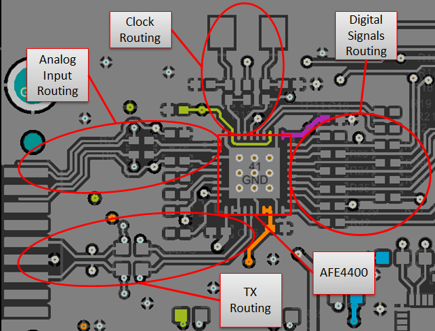
Figure 116. Typical Layout of the AFE4400 Board