ZHCSBO2H December 2012 – July 2014 AFE4400
PRODUCTION DATA.
- 1 特性
- 2 应用
- 3 说明
- 4 修订历史记录
- 5 Device Family Options
- 6 Pin Configuration and Functions
- 7 Specifications
- 8 Detailed Description
- 9 Applications and Implementation
- 10Power Supply Recommendations
- 11Layout
- 12器件和文档支持
- 13机械封装和可订购信息
1 特性
2 应用
- 低成本 医疗脉冲血氧仪应用
- 光学心率监视器 (HRM)
- 工业光测量应用
3 说明
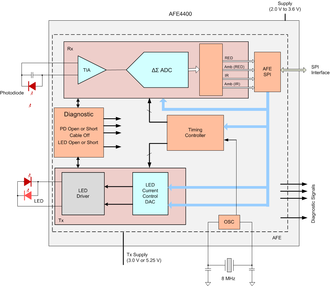
AFE4400 是一款非常适合于脉冲血氧仪应用的完全集成模拟前端 (AFE)。 此器件包含一个具有集成模数转换器 (ADC) 的低噪声接收器通道、一个 LED 发射部件和针对传感器以及 LED 故障检测的诊断功能。 此器件是一款可配置定时控制器。 这个灵活性使得用户能够完全控制器件定时特性。 为了简化计时要求并为 AFE4400 提供一个低抖动时钟,还集成了一个由外部晶振供频的振荡器。 此器件使用一个 SPI™ 接口与外部微控制器或主机处理器通信。
此器件是一个单体、紧凑型 VQFN-40 封装 (6mm x 6mm) 内的完整 AFE 解决方案,其额定工作温度范围为 0°C 至 70°C。
器件信息(1)
| 部件号 | 封装 | 封装尺寸(标称值) |
|---|---|---|
| AFE4400 | VQFN (40) | 6.00mm x 6.00mm |
- 如需了解所有可用封装,请见数据表末尾的可订购产品附录。
4 修订历史记录
Changes from G Revision (July 2014) to H Revision
- Changed HBM value from ±4000 to ±1000 in Handling Ratings table Go
- Changed CDM value from ±1500 to ±250 in Handling Ratings table Go
Changes from F Revision (October 2013) to G Revision
- 已将格式更改为符合最新的数据表标准;已添加全新章节,并已删除现有章节Go
- Changed 发射 特性着重号的子着重号Go
- Changed 集成故障诊断 特性着重号的第二子着重号Go
- Added AFE4403 row to Family and Ordering Information tableGo
- Changed title of Device Family Options tableGo
- Changed INM to INN in VCM description of Pin Descriptions tableGo
- Changed Absolute Maximum Ratings table: changed first five rows and added TXP, TXN pins rowGo
- Deleted Typical value (> 1.3) for Logic high input voltage Go
- Deleted Typical value (> -0.4) for Logic low input voltage Go
- Changed SPISTE, SPISIMO, and SPISOMI pin names in Figure 1Go
- Changed SPISTE and SPISIMO pin names in Figure 2Go
- Added second and third paragraphs to the Receiver Front-End section Go
- Changed seventh paragraph in Receiver Front-End sectionGo
- Changed title of Ambient Cancellation Scheme and Second Stage Gain Block sectionGo
- Changed descriptions of LED2, ambient, and LED1 convert phases in Receiver Control Signals sectionGo
- Changed description of Receiver Timing section Go
- Changed Example column values for rows t2, t4, t5, t11, t13, t15, t17, t19, t22, t24, t26, and t28 in Table 2Go
- Added footnote 2 to Table 2Go
- Added footnote 2 to Figure 42Go
- Added footnote 2 to Figure 43Go
- Changed the ADC Operation and Averaging Module section: grammatical edits and changed the second sentence of the second paragraphGo
- Changed INN pin name in Figure 53Go
- Changed INM to INN in Table 5Go
- Changed SPISTE, SPISIMO, SPISOMI, and SCLK pin names in Figure 58Go
- Added Application and Implementation sectionGo
Changes from E Revision (October 2013) to F Revision
- Changed footnote 1 in Recommended Operating Conditions tableGo
- Changed LED_DRV_SUP parameter in Recommended Operating Conditions tableGo
- Changed TXM to TXN in VLED footnote of Recommended Operating Conditions tableGo
- Changed Transmitter, Voltage on TXP (or TXN) pin parameter in Electrical Characteristics tableGo
- Changed Figure 54 (changed TXP and TXN pin names, deleted LED 1 and LED 2 pin names)Go
Changes from D Revision (May 2013) to E Revision
- Deleted 芯片图Go
- Changed 第 3 特性着重号的第 1 个子着重号Go
- Changed 电源特性着重号的最后一个子着重号Go
- 已更新首页图形Go
- Changed Tx Power Supply column in Family and Ordering Information tableGo
- Changed TX_REF description in Pin Descriptions tableGo
- Changed TX_CTRL_SUP value in Recommended Operating Conditions tableGo
- Changed conditions for Electrical Characteristics tableGo
- Changed Performance, PRF parameter minimum specification in Electrical Characteristics tableGo
- Deleted Performance, IIN_FS parameter from Electrical Characteristics tableGo
- Changed Performance, CMRR parameter in Electrical Characteristics tableGo
- Changed Performance (Full-Signal Chain), Total integrated noise current and NFB parameter test conditions in Electrical Characteristics tableGo
- Changed Receiver Functional Block Level Specification, Total integrated noise current parameter test conditions in Electrical Characteristics tableGo
- Changed Ambient Cancellation Stage, Gain parameter in Electrical Characteristics tableGo
- Added Low-Pass Filter, Filter settling time parameter to Electrical Characteristics tableGo
- Changed Diagnostics, Duration of diagnostics state machine parameter unit value in Electrical Characteristics tableGo
- Changed External Clock, Maximum allowable external clock jitter parameter in Electrical Characteristics tableGo
- Updated Figure 8 to Figure 10Go
- Updated Figure 11 to Figure 16Go
- Updated Figure 17 to Figure 19Go
- Updated Figure 31 and Figure 32Go
- Updated functional block diagramGo
- Updated Figure 34Go
- Changed second sentence in second paragraph of Receiver Front-End sectionGo
- Changed third paragraph of Receiver Front-End sectionGo
- Changed second paragraph of Ambient Cancellation Scheme sectionGo
- Added last paragraph and Table 1 to Ambient Cancellation Scheme sectionGo
- Updated Figure 37Go
- Updated Figure 39Go
- Added footnote 1 to Table 2Go
- Changed example column in Table 2Go
- Added last sentence to third column of row t13 in Table 2Go
- Deleted last sentence from third column of row t14 in Table 2Go
- Changed corresponding register address name in row t21 of Table 2Go
- Updated Figure 42Go
- Updated Figure 43Go
- Updated Figure 44Go
- Changed entire Transmit SectionGo
- Changed second paragraph of the ADC Operation and Averaging Module sectionGo
- Updated Figure 49Go
- Changed Operation section title and first sentenceGo
- Changed last sentence of the Operation With Averaging section Go
- Updated Figure 52Go
- Changed last paragraph of Diagnostics Module sectionGo
- Added first and last sentence to Writing Data sectionGo
- Changed second to last sentence in Writing Data sectionGo
- Added first and last sentence to Reading Data sectionGo
- Changed second to last sentence in Reading Data sectionGo
- Added Multiple Data Reads and Writes sectionGo
- Added last sentence to the AFE SPI Interface Design Considerations sectionGo
- Added Register Control column to Table 6Go
- Changed name of ADCRSTSTCT0 register (address 15h) in Table 6Go
- Changed bit D10 in CONTROL2 row of Table 6Go
- Changed CONTROL0 paragraph descriptionGo
- Added note to bit D2 description of CONTROL0 registerGo
- Corrected bit names in ADCRSTSTCT0 registerGo
- Changed PRPCOUNT[15:0] (bits D[15:0]) description of PRPCOUNT registerGo
- Changed note within CLKALMPIN[2:0] (bits D[11:9]) description of CONTROL1 registerGo
- Changed second and third columns of Table 7Go
- Changed 001 and 011 bit settings for the STG2GAIN[2:0] bits (bits D[10:8]) in the TIA_AMB_GAIN registerGo
- Changed bit D10 of the CONTROL2 registerGo