ZHCS596B December 2011 – June 2019 AFE030
PRODUCTION DATA.
- 1 特性
- 2 应用
- 3 说明
- 4 修订历史记录
- 5 说明(续)
- 6 Pin Configuration and Functions
-
7 Specifications
- 7.1 Absolute Maximum Ratings
- 7.2 ESD Ratings
- 7.3 Thermal Information
- 7.4 Electrical Characteristics: Transmitter (Tx), Tx_DAC
- 7.5 Electrical Characteristics: Transmitter (Tx), Tx_PGA
- 7.6 Electrical Characteristics: Transmitter (Tx), Tx_FILTER
- 7.7 Electrical Characteristics: Power Amplifier (PA)
- 7.8 Electrical Characteristics: Receiver (Rx), Rx PGA1
- 7.9 Electrical Characteristics: Receiver (Rx), Rx Filter
- 7.10 Electrical Characteristics: Receiver (Rx), Rx PGA2
- 7.11 Electrical Characteristics: Digital
- 7.12 Electrical Characteristics: Two-Wire Interface
- 7.13 Electrical Characteristics: Zero-Crossing Detector
- 7.14 Electrical Characteristics: Internal Bias Generator
- 7.15 Electrical Characteristics: Power Supply
- 7.16 Typical Characteristics
- 8 Parameter Measurement Information
- 9 Detailed Description
- 10Application and Implementation
- 11器件和文档支持
9.3.4 DAC Block
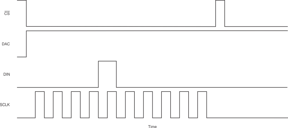
The DAC block consists only of the 10-bit DAC. The use of the DAC is recommended for best performance. The serial interface is used to write directly to the DAC registers when the DAC pin (pin 7) is driven high. Placing the DAC pin into a high state configures the SPI for direct serial interface to the DAC. Use the following sequence to write to the DAC:
- Set CS low.
- Set the DAC pin (pin 7) high.
- Write a 10-bit word to DIN. The DAC register is left-justified and truncates more than 10 bits.
- CS high updates the DAC.
Refer to Figure 35 for an illustration of this sequence.
 Figure 35. Writing to the DAC Register
 Table 7 lists the DAC Register configurations.
Table 7. DAC Registers
| DAC PIN HIGH:
DAC REGISTER <15:0> |
LOCATION
(0 = LSB) |
DEFAULT | R/W | FUNCTION |
|---|---|---|---|---|
| BIT NAME | ||||
| DAC<0> | 0 | — | W | Truncated |
| DAC<1> | 1 | — | W | Truncated |
| DAC<2> | 2 | — | W | Truncated |
| DAC<3> | 3 | — | W | Truncated |
| DAC<4> | 4 | — | W | Truncated |
| DAC<5> | 5 | — | W | Truncated |
| DAC<6> | 6 | — | W | DAC bit 0 = DAC LSB |
| DAC<7> | 7 | — | W | DAC bit 1 |
| DAC<8> | 8 | — | W | DAC bit 2 |
| DAC<9> | 9 | — | W | DAC bit 3 |
| DAC<10> | 10 | — | W | DAC bit 4 |
| DAC<11> | 11 | — | W | DAC bit 5 |
| DAC<12> | 12 | — | W | DAC bit 6 |
| DAC<13> | 13 | — | W | DAC bit 7 |
| DAC<14> | 14 | — | W | DAC bit 8 |
| DAC<15> | 15 | — | W | DAC bit 9 = DAC MSB |