ZHCSIJ5C August 2018 – June 2019 ADS9224R , ADS9234R
PRODUCTION DATA.
- 1 特性
- 2 应用
- 3 说明
- 4 修订历史记录
- 5 Pin Configuration and Functions
-
6 Specifications
- 6.1 Absolute Maximum Ratings
- 6.2 ESD Ratings
- 6.3 Recommended Operating Conditions
- 6.4 Thermal Information
- 6.5 Electrical Characteristics: ADS92x4R
- 6.6 Electrical Characteristics: ADS9224R
- 6.7 Electrical Characteristics: ADS9234R
- 6.8 Timing Requirements
- 6.9 Switching Characteristics
- 6.10 Typical Characteristics: ADS9224R
- 6.11 Typical Characteristics: ADS9234R
-
7 Detailed Description
- 7.1 Overview
- 7.2 Functional Block Diagram
- 7.3 Feature Description
- 7.4 Device Functional Modes
- 7.5 READY/STROBE Output
- 7.6
Programming
- 7.6.1 Output Data Word
- 7.6.2
Data Transfer Protocols
- 7.6.2.1
Protocols for Reading From the Device
- 7.6.2.1.1 Legacy, SPI-Compatible Protocols (SPI-xy-S-SDR)
- 7.6.2.1.2 SPI-Compatible Protocols With Bus Width Options and Single Data Rate (SPI-xy-D-SDR and SPI-xy-Q-SDR)
- 7.6.2.1.3 SPI-Compatible Protocols With Bus Width Options and Double Data Rate (SPI-x1-S-DDR, SPI-x1-D-DDR, SPI-x1-Q-DDR)
- 7.6.2.1.4 Clock Re-Timer (CRT) Protocols (CRT-S-SDR, CRT-D-SDR, CRT-Q-SDR, CRT-S-DDR, CRT-D-DDR, CRT-Q-DDR)
- 7.6.2.1.5 Parallel Byte Protocols (PB-xy-AB-SDR, PB-xy-AA-SDR)
- 7.6.2.2 Device Setup
- 7.6.2.3 Protocols for Configuring the Device
- 7.6.2.1
Protocols for Reading From the Device
- 7.6.3 Reading and Writing Registers
- 7.7
Register Maps
- 7.7.1
ADS92x4R Registers
- 7.7.1.1 DEVICE_STATUS Register (Offset = 0h) [reset = 0h]
- 7.7.1.2 POWER_DOWN_CFG Register (Offset = 1h) [reset = 0h]
- 7.7.1.3 PROTOCOL_CFG Register (Offset = 2h) [reset = 0h]
- 7.7.1.4 BUS_WIDTH Register (Offset = 3h) [reset = 0h]
- 7.7.1.5 CRT_CFG Register (Offset = 4h) [reset = 0h]
- 7.7.1.6 OUTPUT_DATA_WORD_CFG Register (Offset = 5h) [reset = 0h]
- 7.7.1.7 DATA_AVG_CFG Register (Offset = 6h) [reset = 0h]
- 7.7.1.8 REFBY2_OFFSET Register (Offset = 7h) [reset = 0h]
- 7.7.1
ADS92x4R Registers
- 8 Application and Implementation
- 9 Power Supply Recommendations
- 10Layout
- 11器件和文档支持
- 12机械、封装和可订购信息
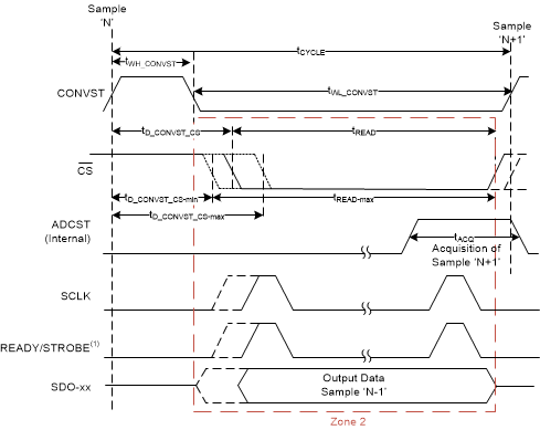
7.4.4.2 Conversion Control and Data Transfer Frame With Wide Read Cycle (Zone 2 Transfer)
In this mode of conversion control and data transfer, the device starts conversion on the rising edge of CONVST. The CONVST pin can be pulled low after a minimum time of tWH_CONVST. After a time of tD_CONVST_CS (see tD_CONVST_CS for zone 2 transfer in the Specifications section), the host must pull CS low and provide clocks on the SCLK pin to read the data in zone 2. As shown in Figure 45, a zone 2 transfer provides more read time (tread). The read time available for reading data is maximized when tD_CONVST_CS is set to the minimum permissible value. The data for the previous sample (sample N-1) is provided by the device on the SDO pins. After all bits are read, the host can pull the CS pin high to end the data transfer frame. After pulling CS high, the host can pull the CONVST pin high to start the next conversion. In this mode of conversion control, a minimum time of tCYCLE (see tCYCLE for zone 2 transfer in the Specifications section) is required between two adjacent rising edges of the CONVST signal. The host must keep the SDI pin low (NOP0) or high (NOP1) for conversion control and for getting conversion results from the device.

NOTE
For optimum performance with zone 2 transfer, TI recommends masking the READY output by setting the READY_MASK bit in the OUTPUT_DATA_WORD_CFG register and using a data transfer protocol with a bus width of more than 2 SDOs or the parallel byte protocol to keep [tD_CONVST_CS + tREAD] below 150 ns. See the Protocols for Reading From the Device section for details on different protocols for reading the data.