SBAS363E December 2009 – August 2016 ADS8331 , ADS8332
PRODUCTION DATA.
- 1 Features
- 2 Applications
- 3 Description
- 4 Revision History
- 5 Companion Products
- 6 Device Comparison
- 7 Pin Configuration and Functions
-
8 Specifications
- 8.1 Absolute Maximum Ratings
- 8.2 ESD Ratings
- 8.3 Recommended Operating Conditions
- 8.4 Thermal Information
- 8.5 Electrical Characteristics: VA = 2.7 V
- 8.6 Electrical Characteristics: VA = 5 V
- 8.7 Timing Requirements: VA = 2.7 V
- 8.8 Timing Characteristics: VA = 5 V
- 8.9 Typical Characteristics: DC Performance
- 8.10 Typical Characteristics: AC Performance
- 9 Detailed Description
- 10Application and Implementation
- 11Power Supply Recommendations
- 12Layout
- 13Device and Documentation Support
- 14Mechanical, Packaging, and Orderable Information
封装选项
机械数据 (封装 | 引脚)
散热焊盘机械数据 (封装 | 引脚)
- RGE|24
订购信息
9 Detailed Description
9.1 Overview
The ADS833x is a high-speed, low-power, successive approximation register (SAR) analog-to-digital converter (ADC) that uses an external reference. The architecture is based on charge redistribution, which inherently includes a sample/hold function.
The ADS833x has an internal clock that is used to run the conversion. However, the ADS833x can be programmed to run the conversion based on the external serial clock (SCLK).
The analog input to the ADS833x is provided to two input pins: one of the INX input channels and the shared COM pin. When a conversion is initiated, the differential input on these pins is sampled on the internal capacitor array. While a conversion is in progress, both INX and COM inputs are disconnected from any internal function.
The ADS8331 has four analog inputs while the ADS8332 has eight inputs. All inputs share the same common pin, COM. Both the ADS8331 and ADS8332 can be programmed to select a channel manually or can be programmed into the auto channel select mode to sweep through the input channels automatically.
9.2 Functional Block Diagram

9.3 Feature Description
9.3.1 Signal Conditioning
The ADS833x has the flexibility to add signal conditioning between the MUXOUT and ADCIN pins, such as a programmable gain amplifier (PGA) or filter. This feature reduces the system component count and cost because each input channel does not require separate signal conditioning circuits, especially if the source impedance connected to each channel is similar in value.
9.3.2 Analog Input
When the converter enters the hold mode, the voltage difference between the INX and COM inputs is captured on the internal capacitor array. The voltage on the COM pin is limited from (AGND – 0.2 V) to (AGND + 0.2 V). This limitation allows the ADS833x to reject small signals that are common to both the INX and COM inputs. The INX inputs have a range of –0.2 V to (VA + 0.2 V). The input span of (INX – COM) is limited to 0 V to VREF.
The peak input current through the analog inputs depends upon a number of factors: reference voltage, sample rate, input voltage, and source impedance. The current flowing into the ADS833x charges the internal capacitor array during the sample period. After this capacitance has been fully charged, there is no further input current. The source of the analog input voltage must be able to charge the maximum input capacitance (45 pF) to a 16-bit settling level within the minimum acquisition time (238 ns). When the converter goes into hold mode, the input impedance is greater than 1 GΩ.
Take care when regarding the absolute analog input voltage. To maintain linearity of the converter, the INX inputs, the COM input, and the input span of (INX – COM) should be within the limits specified. If these inputs are outside of these ranges, the linearity of the converter may not meet specifications. To minimize noise, low-bandwidth input signals with low-pass filters should be used. Ensure that the output impedance of the sources driving the INX and COM inputs are matched, as shown in Figure 34. If this matching is not observed, the two inputs could have different settling times, which may result in an offset error, gain error, and linearity error that change with temperature and input voltage.
9.3.2.1 Driver Amplifier Choice
To take advantage of the high sample rate offered by the ADS833x, the analog inputs to the converter should be driven with low-noise operational amplifiers (op amps), such as the OPA365, OPA211, OPA827, or THS4031. TI recommends a RC filter at each of the input channels to low-pass filter noise generated by the input driving sources. These channels can accept unipolar signals with voltages between INX and COM in the range of 0 V to VREF. If RC filters are not used between the op amps and the input channels, the minimum –3-dB bandwidth required by the driving op amps for the sampled signals to settle to within 1/2 LSB of the final voltage can be calculated using Equation 1:

where
- n = resolution of the converter (n = 16 for the ADS833x).
- tSAMPLE_MIN = minimum acquisition time.
The minimum value of tSAMPLE in Electrical Characteristics: VA = 2.7 V and Electrical Characteristics: VA = 5 V is 238 ns (3 CCLKs with the internal oscillator at 12.6 MHz). Substituting these values for n and tSAMPLE_MIN into Equation 1 shows f–3 dB must be at least 7.9 MHz. This bandwidth can be relaxed if the acquisition time is increased or an RC filter is added between the driving operational amplifier and the corresponding input channel (see Texas Instruments' Application Report, Determining Minimum Acquisition Times for SAR ADCs When a Step Function is Applied to the Input (SBAA173) and associated references for additional information, available for download at www.ti.com). The OPA365 used in the source-follower (unity-gain) configuration is shown in Figure 35 with recommended values for the RC filter.
 Figure 35. Unipolar Input Drive Configuration
9.3.2.2 Bipolar to Unipolar Driver
In systems where the input signal is bipolar, op amps such as the OPA365 and OPA211 can be used in the inverting configuration with a DC bias applied to the noninverting input to keep the input signal to the ADS833x within its rated operating voltage range. TI also recommends this configuration when the ADS833x is used in signal-processing applications where good SNR and THD performance is required. The DC bias can be derived from low-noise reference voltage ICs such as the REF5025 or REF5040. The input configuration shown in Figure 36 is capable of delivering better than 91-dB SNR and –99-dB THD at an input frequency of 1 kHz. If bandpass filters are used to filter the input to the driving operational amplifier, the signal swing at the input of the bandpass filter should be small enough to minimize the distortion introduced by the filter. In these cases, the gain of the circuit shown in Figure 36 can be increased to maintain a large enough input signal to the ADS833x to keep the system SNR as high as possible.
 Figure 36. Bipolar Input Drive Configuration
9.4 Device Functional Modes
9.4.1 Reference
The ADS833x can operate with an external reference with a range from 1.2 V to 4.2 V. A clean, low-noise reference voltage on this pin is required to ensure good converter performance. A low-noise band-gap reference such as the REF5025 or REF5040 can be used to drive this pin. A 10-μF ceramic bypass capacitor is required between the REF+ and REF– pins of the converter. This capacitor should be placed as close as possible to the pins of the device. The REF– pin should not be connected to the AGND pin of the converter; instead, the REF– pin must be connected to the analog ground plane with a separate via.
9.4.2 Converter Operation
The ADS833x has an internal oscillator that can be used as the conversion clock (CCLK) source. The minimum frequency of this oscillator is 10.5 MHz. The internal oscillator is only active during the conversion period unless the converter is using Auto-Trigger or Auto-NAP modes. The minimum acquisition, sampling time for the ADS833x is 3 CCLKs (250 ns with a 12-MHz conversion clock), while the minimum conversion time is 18 CCLKs (1500 ns with a 12-MHz conversion clock).
As shown in Figure 37, the ADS833x can also be programmed to run conversions using the external serial clock (SCLK). This feature allows system designers to achieve system synchronization. Each rising edge of SCLK toggles the state of the conversion clock (CCLK), which reduces the frequency of SCLK by a factor of two before it is used as CCLK. For example, a 21-MHz SCLK provides a 10.5-MHz CCLK. If the start of a conversion must occur on a specific rising edge of SCLK when the external serial clock is used for the conversion clock (and Manual-Trigger mode is enabled), a minimum setup time of 20 ns between the falling edge of CONVST and the rising edge of SCLK must be met. This timing ensures the conversion is completed in 18 CCLKs (36 SCLKs).
The duty cycle of SCLK is not critical, as long as the minimum high and low times (11 ns for VA = 5 V) are satisfied. Because the ADS833x is designed for high-speed applications, a high-frequency serial clock must be supplied to maintain the high throughput of the interface. This requirement can be accomplished if the period of SCLK is at most 1 μs when SCLK is used as the conversion clock (CCLK). The 1-μs maximum period for SCLK is also set by the leakage of charge from the capacitors in the capacitive digital-to-analog converter (CDAC) block in the ADS833x. If SCLK is used as the conversion clock, the SCLK source must have minimal rise, fall times and low jitter to provide the best converter performance.
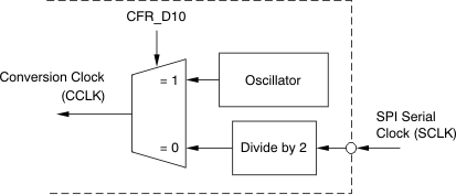 Figure 37. Conversion Clock Source
9.4.2.1 Manual Channel Select Mode
Manual Channel Select mode is enabled through the Configuration register (CFR) by setting the CFR_D11 bit to 0 (see Table 5). The acquisition process starts with selecting an input channel. This selection is done by writing the desired channel number to the Command register (CMR); see Table 4 for further details. The associated timing diagram is shown in Figure 38.
 Figure 38. Manual Channel Select Timing
9.4.2.2 Auto Channel Select Mode
Channel selection can also be done automatically if Auto Channel Select mode (default) is enabled (CFR_D11 = 1). If the device is programmed for Auto Channel Select mode, then signals from all channels are acquired in a fixed order. In Auto Channel Select mode, the first conversion after entering this mode is always from the channel of the last conversion completed before this mode is enabled. The channels are then sequentially scanned up to and including the last channel (that is, channel 3 for the ADS8331 and channel 7 for the ADS8332) and then back to the channel that started the sequence. For example, if the last channel used in the conversion before enabling Auto Channel Select mode was channel 2, the sequence for the ADS8332 would be: 2, 3, 4, 5, 6, 7, 2, and so forth, as shown in Figure 39. If the last channel in Manual Channel Select mode happened to be channel 7, the sequence would be: 7, 7, 7, and so forth. Figure 40 shows when the next channel in the sequence activates during Auto Channel Select mode. This timing allows the next channel to settle before it is acquired. This automatic sequencing stops the cycle after CFR_D11 is set to 0.
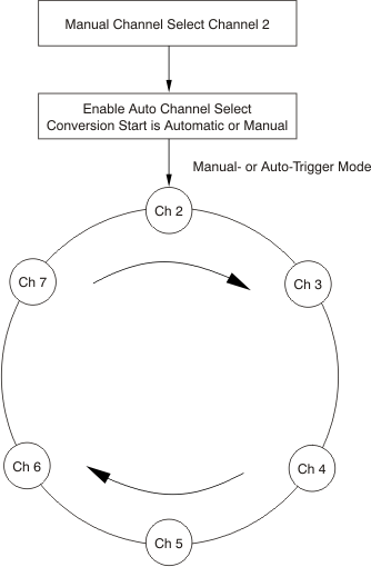 Figure 39. Auto Channel Select for the ADS8332
 Figure 40. Channel-Number Update in Auto Channel Select Mode Timing
9.4.2.3 Start of a Conversion
The end of acquisition is the same as the start of a conversion. This process is initiated by bringing the CONVST pin low for a minimum of 40 ns. After the minimum requirement has been met, the CONVST pin can be brought high. CONVST acts independently of FS/CS so it is possible to use one common CONVST for applications that require simultaneous sample/hold with multiple converters. The ADS833x switches from sample to hold mode on the falling edge of the CONVST signal. The ADS833x requires 18 conversion clock (CCLK) cycles to complete a conversion. The conversion time is equivalent to 1500 ns with a 12-MHz internal clock. The minimum time between two consecutive CONVST signals is 21 CCLKs.
A conversion can also be initiated without using CONVST if the ADS833x is programmed for Auto-Trigger mode (CFR_D9 = 0). When the converter is configured in this mode, and with CFR_D8 = 0, the next conversion is automatically started three conversion clocks (CCLK) after the end of a conversion. These three conversion clocks (CCLK) are used for the acquisition time. In this case, the time to complete one acquisition and conversion cycle is 21 CCLKs. Table 1 summarizes the different conversion modes.
Table 1. Different Types of Conversion
| MODE | SELECT CHANNEL | START CONVERSION |
|---|---|---|
| Automatic | Auto Channel Select(1) | Auto-Trigger Mode |
| No need to write channel number to CMR. Use internal sequencer for ADS833x. | Start a conversion based on conversion clock CCLK | |
| Manual | Manual Channel Select | Manual-Trigger Mode |
| Write channel number to CMR | Start a conversion with CONVST |
Manual Channel select with Auto-Trigger mode enabled is generally used when continuous conversions from a single channel are desired. In this mode, cycling the input mux to change the channel requires that conversions are halted by setting the converter to Manual-Trigger mode. When the proper input channel is selected, the converter can be placed back to Auto-Trigger mode to continue continuous conversions from the new channel.
9.4.2.4 Status Output Pin (EOC/INT)
The status output pin is programmable. It can be used as an EOC output (CFR_D[7:6] = 11) where the low time is equal to the conversion time. When the status pin is programmed as EOC and the polarity is set as active low, the pin works in the following manner: the EOC output goes low immediately following CONVST going low with Manual-Trigger mode enabled. EOC stays low throughout the conversion process and returns high when the conversion has ended. If Auto-Trigger mode is enabled, the EOC output remains high for three conversion clocks (CCLK) after the previous rising edge of EOC.
This status pin can also be used as an interrupt output, INT (CFR_D[7:6] = 10), which is set low at the end of a conversion, and is brought high (cleared) by the next read cycle. The polarity of this pin, whether used as EOC or INT, is programmable through the CFR_D7 bit.
9.4.2.5 Power-Down Modes and Acquisition Time
There are three power-down modes that reduce power dissipation: Nap, Deep, and Auto-NAP. The first two, Nap and Deep Power-Down modes, are enabled or disabled by bits CFR_D3 and CFR_D2, respectively, in the Configuration register (see Table 5 for details).
Deep Power-Down mode provides maximum power savings. When this mode is enabled, the analog core in the converter is shut down, and the analog supply current falls from 6.6 mA (VA = 5 V) to 1 μA in 2 μs. The wake-up time from Deep Power-Down mode is 1 μs. The device can wake up from Deep Power-Down mode by either disabling this mode, issuing the wake-up command, loading the default value into the CFR, or performing a reset (either with the software reset command, CFR_D0 bit, or the external reset). See Table 4 and Table 5 along with the section for further information.
In Nap Power-Down mode, the bias currents for the analog core of the device are significantly reduced. Because the bias currents are not completely shut off, the ADS833x can wake up from this power-down mode much faster than from Deep Power-Down mode. After Nap Power-Down mode is enabled, the analog supply current falls from 6.6 mA (VA = 5 V) to 0.39 mA in 200 ns. The wake-up time from this mode is three conversion clock cycles (CCLK). The device can wake up from Nap Power-Down mode in the same manner as waking up from Deep Power-Down mode.
The third power-down mode, Auto-NAP, is enabled or disabled by bit CFR_D4 in the Configuration register (see Table 5 for details). Once this mode is enabled, the device is controlled by the digital core logic on the chip. The device is automatically placed into Nap Power-Down mode after the next end of conversion (EOC). The analog supply current falls from 6.6mA (VA = 5 V) to 0.39 mA in 200 ns. A conversion start wakes up the device in three conversion clock cycles. Issuing the wake-up command, loading the default value into the CFR, disabling Auto-NAP Power-Down mode, issuing a manual channel select command, or resetting the device can wake the ADS833x from Auto-NAP Power-Down mode. A comparison of the three power-down modes is listed in Table 2.
Table 2. Comparison of Power-Down Modes
| TYPE OF POWER-DOWN | POWER CONSUMPTION (VA = 5 V) |
POWER-DOWN BY: | POWER-DOWN TIME | WAKEUP BY: | WAKE-UP TIME | ENABLE |
|---|---|---|---|---|---|---|
| Normal operation | 6.6 mA | — | — | — | — | — |
| Deep power-down | 1 μA | Setting CFR_D2 | 2 μs | Wakeup command 1011b | 1 μs | Set CFR_D2 |
| Nap power-down | 0.39 mA | Setting CFR_D3 | 200 ns | Wakeup command 1011b | 3 CCLKs | Set CFR_D3 |
| Auto-NAP power-down | 0.39 mA | EOC (end of conversion) | 200 ns | CONVST, any channel select command, default command 1111b, or wakeup command 1011b. | 3 CCLKs | Set CFR_D4 |
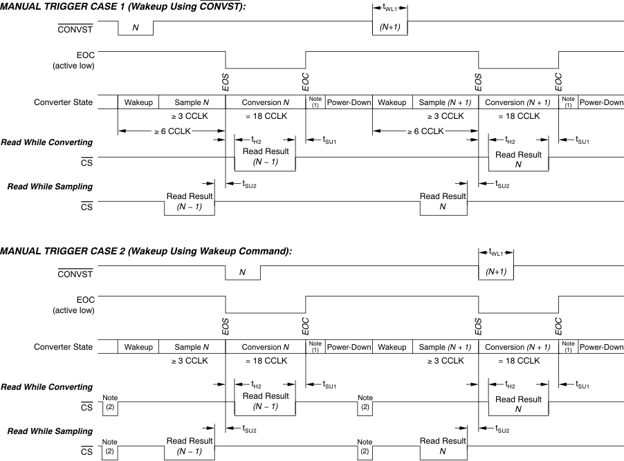
The default acquisition time is three conversion clock (CCLK) cycles. Figure 41 shows the timing diagram for CONVST, EOC, and Auto-NAP power-down signals in Manual-Trigger mode. As shown in the diagram, the device wakes up after a conversion is triggered by the CONVST pin going low. However, a conversion is not yet started at this time. The conversion start signal to the analog core of the chip is internally generated no less than six conversion clock (CCLK) cycles later, to allow at least three CCLKs for wake up and three CCLKs for acquisition. The ADS833x enters Nap Power-Down mode one conversion cycle after the end of conversion (EOC).
 Figure 41. Timing for CONVST, EOC, and Auto-NAP Power-Down Signals in Manual-Trigger Mode (Three Conversion Clock Cycles for Acquisition)
The ADS833x can support sampling rates of up to 500 kSPS in Auto-Trigger mode. This rate is selectable by programming the CFR_D8 bit in the Configuration register. In 500-kSPS mode, consecutive conversion start pulses to the analog core are generated 21 conversion clock cycles apart. In 250-kSPS mode, consecutive conversion-start pulses are 42 conversion clock cycles apart. The Nap and Deep Power-Down modes are available with either sampling rate; however, Auto-NAP mode is available only with a sampling rate of 250 kSPS when Auto-Trigger mode is enabled. The analog core cannot be powered down when the Auto-NAP mode sampling rate is 500 kSPS because at that rate, there is no period of time when the analog core is not actively being used.
Figure 42 shows the timing diagram for conversion start and Auto-NAP power-down signals for a 250-kSPS sampling rate in Auto-Trigger mode. For a 16-bit ADC output word, consecutive new conversion start pulses are generated 2 × (18 + 3) cycles apart. NAP_ACTIVE (the signal to power down the analog core in Nap and Auto-NAP modes) goes low six (3 + 3) conversion clock cycles before the conversion start falling edge, thus powering up the analog core. It takes three conversion clock cycles after NAP_ACTIVE goes low to power up the analog core. The analog core is powered down a cycle after the end of a conversion. For a 16-bit ADC with a 500-kSPS sampling rate and three conversion clock cycle sampling, consecutive conversion start pulses are generated 21 conversion clock cycles apart.
 Figure 42. Timing for Conversion Start and Auto-NAP Power-Down Signals in Auto-Trigger Mode (250-kSPS Sampling and Three Conversion Clock Cycles for Acquisition)
Timing diagrams for reading from the ADS833x with various trigger and power-down modes are shown in Figure 43 through Figure 45. The total (acquisition + conversion) times for the different trigger and power-down modes are listed in Table 3.
Table 3. Total Acquisition + Conversion Times
| MODE | ACQUISITION + CONVERSION TIME |
|---|---|
| Auto-Trigger at 500 kSPS | = 21 CCLK |
| Manual-Trigger | ≥ 21 CCLK |
| Manual-Trigger with Deep Power Down | ≥ 4 SCLK + 1 μs + 3 CCLK + 18 CCLK + 16 SCLK + 2 μs |
| Manual-Trigger with Nap Power Down | ≥ 4 SCLK + 3 CCLK + 3 CCLK + 18 CCLK + 16 SCLK + 200 ns |
| Manual-Trigger with Auto-NAP Power Down | ≥ 4 SCLK + 3 CCLK + 3 CCLK + 18 CCLK + 1 CCLK + 200 ns (using wakeup to resume) |
| ≥ 3 CCLK + 3 CCLK + 18 CCLK + 1 CCLK + 200 ns (using CONVST to resume) |
 Figure 43. Read While Converting vs Read While Sampling (Manual-Trigger Mode)
BLANKSPACE

(Manual-Trigger Mode)
9.5 Programming
9.5.1 Digital Interface
The serial interface is designed to accommodate the latest high-speed processors with an SCLK frequency of up to 40 MHz (VA = VBD = 5 V). Each cycle starts with the falling edge of FS/CS. The internal data register content, which is made available to the output register at the end of conversion, is presented on the SDO output pin on the falling edge of FS/CS. The first bit is the most significant bit (MSB). The output data bits are valid on the falling edge of SCLK with the tD2 delay (see the Timing Requirements: VA = 2.7 V and Timing Characteristics: VA = 5 V) so that the host processor can read the data on the falling edge. Serial data input is also read on the falling edge of SCLK.
The complete serial I/O cycle starts after the falling edge of FS/CS and ends 16 falling edges of SCLK later (see NOTE). The serial interface works with CPOL = 1, CPHA = 0. This setting means the falling edge of FS/CS may fall while SCLK is high. The same timing relaxation applies to the rising edge of FS/CS where SCLK may be high or low as long as the last SCLK falling edge happens before the rising edge of FS/CS.
NOTE
There are cases where a cycle can be anywhere from 4 SCLKs up to 24 SCLKs, depending on the read mode combination. See Table 4 for details.
9.5.1.1 Internal Register
The internal register consists of two parts: four bits for the Command register (CMR) and 12 bits for the Configuration register (CFR).
Table 4. Command Set Defined by Command Register (CMR)(1)
| D[15:12] | HEX | COMMAND | D[11:0] | WAKE UP FROM AUTO-NAP | MINIMUM SCLKs REQUIRED | R/W | |
|---|---|---|---|---|---|---|---|
| 0000b | 0h | Select analog input channel 0 | Don't care | Y | 4 | W | |
| 0001b | 1h | Select analog input channel 1 | Don't care | Y | 4 | W | |
| 0010b | 2h | Select analog input channel 2 | Don't care | Y | 4 | W | |
| 0011b | 3h | Select analog input channel 3 | Don't care | Y | 4 | W | |
| 0100b | 4h | Select analog input channel 4(2) | Don't care | Y | 4 | W | |
| 0101b | 5h | Select analog input channel 5(2) | Don't care | Y | 4 | W | |
| 0110b | 6h | Select analog input channel 6(2) | Don't care | Y | 4 | W | |
| 0111b | 7h | Select analog input channel 7(2) | Don't care | Y | 4 | W | |
| 1000b | 8h | Reserved | Reserved | — | — | — | |
| 1001b | 9h | Reserved | Reserved | — | — | — | |
| 1010b | Ah | Reserved | Reserved | — | — | — | |
| 1011b | Bh | Wake up | Don't care | Y | 4 | W | |
| 1100b | Ch | Read CFR | Don't care | — | 16 | R | |
| 1101b | Dh | Read data | Don't care | — | 16 | R | |
| 1110b | Eh | Write CFR | CFR Value | — | 16 | W | |
| 1111b | Fh | Default mode (load CFR with default value) |
Don't care | Y | 4 | W | |
9.5.2 Writing to the Converter
There are two different types of writes to the register: a 4-bit write to the CMR and a full 16-bit write to the CMR plus CFR. The command set is listed in Table 4 and the configuration register map is listed in Table 5. A simple command requires only four SCLKs; the write takes effect on the fourth falling edge of SCLK. A 16-bit write or read takes at least 16 SCLKs (see Table 7 for exceptions that require more than 16 SCLKs).
9.5.2.1 Configuring the Converter and Default Mode
The converter can be configured with command 1110b (write to the CFR) or command 1111b (default mode). A write to the CFR requires a 4-bit command followed by 12 bits of data. A 4-bit command takes effect on the fourth falling edge of SCLK. A write to the CFR takes effect on the 16th falling edge of SCLK.
The CFR default value for each bit is 1. The default values are applied to the CFR after issuing command 1111b or when the device is reset with a power-on reset (POR), software reset, or external reset using the RESET pin (see the Reset Function section).
The communication protocol of the ADS833x is full duplex. That is, data are transmitted to and from the device simultaneously. For example, the input mux channel can be changed via the SDI pin while data are being read through the SDO pin. All commands, except Read CFR, output conversion data on the SDO pin. If a Read CFR command is issued, the Read Data command can then be used to read back the conversion result.
9.5.3 Reading the Configuration Register
The host processor can read back the value programmed in the CFR by issuing command 1100b. The timing is similar to reading a conversion result except CONVST is not used. There is also no activity on the EOC/INT pin. The CFR value readback contains the first four bits (MSBs) of the previous conversion data plus the 12-bit CFR contents.
Table 5. Configuration Register (CFR) Map
| CFR SDI BIT (Default = FFFh) |
DEFINITION | BIT = 0 | BIT = 1 | |
|---|---|---|---|---|
| D11 | Channel select mode | Manual channel select enabled. Use channel select commands to access a desired channel. | Auto channel select enabled. Channels are sampled and converted sequentially until the cycle after this bit is set to 0. | |
| D10 | Conversion clock (CCLK) source select | Conversion clock (CCLK) = SCLK / 2 | Conversion clock (CCLK) = internal OSC | |
| D9 | Trigger (conversion start) select: start conversion at the end of sampling (EOS). If D9 = 0 and D8 = 0, the D4 setting is ignored. | Auto-Trigger: conversions automatically start three conversion clocks after EOC at 500 kSPS | Manual-Trigger: conversions manually start on falling edge of CONVST | |
| D8 | Sample rate for Auto-Trigger mode | 500kSPS (21 CCLKs) | 250 kSPS (42 CCLKs) | |
| D7 | Pin 10 polarity select when used as an output (EOC/INT) | EOC/INT active high | EOC/INT active low | |
| D6 | Pin 10 function select when used as an output (EOC/INT) | Pin used as INT | Pin used as EOC | |
| D5 | Pin 10 I/O select for daisy-chain mode operation | Pin 10 is used as CDI input (daisy-chain mode enabled) |
Pin 10 is used as EOC/INT output | |
| D4 | Auto-NAP Power-Down enable or disable. This bit setting is ignored if D9 = 0 and D8 =0. | Auto-NAP Power-Down mode enabled (not activated) | Auto-NAP Power-Down mode disabled | |
| D3 | Nap Power Down. This bit is set to 1 automatically by wake-up command. | Nap Power-Down enabled | Nap Power-Down disabled (resume normal operation) |
|
| D2 | Deep Power Down. This bit is set to 1 automatically by wake-up command. | Deep Power-Down enabled | Deep Power-Down disabled (resume normal operation) |
|
| D1 | TAG bit output enable | TAG bit output disabled | TAG bit output enabled. TAG bits appear after conversion data | |
| D0 | Software reset | System reset, returns to 1 automatically | Normal operation | |
9.5.4 Reading the Conversion Result
The conversion result is available to the input of the output data register (ODR) at EOC and presented to the output of the output register at the next falling edge of FS/CS. The host processor can then shift the data out through the SDO pin at any time except during the quiet zone. This duration is 20 ns before and 20 ns after the end of sampling (EOS) period. End of sampling (EOS) is defined as the falling edge of CONVST when Manual-Trigger mode is used or the end of the third conversion clock (CCLK) after EOC if Auto-Trigger mode is used.
The falling edge of FS/CS should not be placed at the precise moment at the end of a conversion (by default when EOC goes high). Otherwise, the data could be corrupt. If FS/CS is placed before the end of a conversion, the previous conversion result is read. If FS/CS is placed after the end of a conversion, the current conversion result is read.
The conversion result is 16-bit data in straight binary format as shown in Table 6. Generally 16 SCLKs are necessary, but there are exceptions when more than 16 SCLKs are required (see Table 7). Data output from the serial output (SDO) is left-adjusted MSB first. The trailing bits are filled with three TAG bits first (if enabled) plus all 0s. SDO remains low until FS/CS is brought high again.
SDO is active when FS/CS is low. The rising edge of FS/CS 3-states the SDO output.
NOTE
Whenever SDO is not in 3-state (that is, when FS/CS is low and SCLK is running), a portion of the conversion result is output at the SDO pin. The number of bits depends on how many SCLKs are supplied. For example, a manual channel select command cycle requires 4 SCLKs. Therefore, four MSBs of the conversion result are output at SDO. The exception is when SDO outputs all 1s during the cycle immediately after any reset (POR, software reset, or external reset).
If SCLK is used as the conversion clock (CCLK) and a continuous SCLK is used, it is not possible to clock out all 16 bits from SDO during the sampling time (6 SCLKs) because of the quiet zone requirement. In this case, it is better to read the conversion result during the conversion time (36 SCLKs or 48 SCLKs in Auto-NAP mode).
Table 6. Ideal Input Voltages and Output Codes
| DESCRIPTION | ANALOG VALUE | DIGITAL OUTPUT | |
|---|---|---|---|
| STRAIGHT BINARY | |||
| BINARY CODE | HEX CODE | ||
| Full-scale range | VREF | — | — |
| Least significant bit (LSB) | VREF / 65536 | — | — |
| Full-scale | VREF – 1 LSB | 1111 1111 1111 1111 | FFFF |
| Midscale | VREF / 2 | 1000 0000 0000 0000 | 8000 |
| Midscale – 1 LSB | VREF / 2– 1 LSB | 0111 1111 1111 1111 | 7FFF |
| Zero | 0 V | 0000 0000 0000 0000 | 0000 |
9.5.4.1 TAG Mode
The ADS833x includes a TAG feature that can be used to indicate which channel sourced the converted result. If TAG mode is enabled, three address bits are added after the LSB of the conversion data is read out from SDO to indicate which channel corresponds to the result. These address bits are 000 for channel 0, 001 for channel 1, 010 for channel 2, 011 for channel 3, 100 for channel 4, 101 for channel 5, 110 for channel 6, and 111 for channel 7. The converter requires at least 19 SCLKs when TAG mode is enabled to transfer the 16-bit conversion result and the three TAG bits.
9.5.4.2 Daisy-Chain Mode
The ADS833x can operate as a single converter or in a system with multiple converters. System designers can take advantage of the simple, high-speed, SPI-compatible serial interface by cascading converters in a single chain when multiple converters are used. The CFR_D5 bit in the Configuration register is used to reconfigure the EOC/INT status pin as the chain data input (CDI) pin, a secondary serial data input, for the conversion result from an upstream converter. This configuration is called daisy-chain mode operation. A typical connection of three converters in daisy-chain mode is shown in Figure 46.
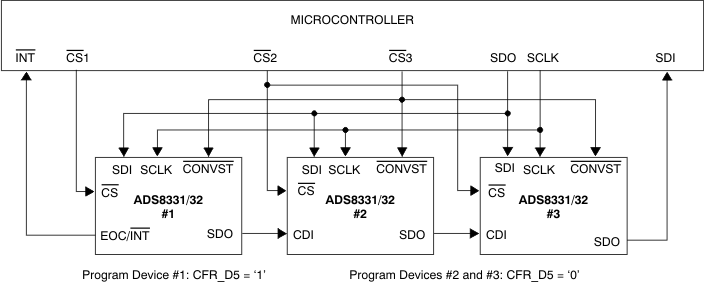 Figure 46. Multiple Converters Connected Using Daisy-Chain Mode
When multiple converters are used in daisy-chain mode, the first converter is configured in regular mode while the rest of the converters downstream are configured in daisy-chain mode. When a converter is configured in daisy-chain mode, the CDI input data go straight to the output register. Therefore, the serial input data passes through the converter with either a 16 SCLK (if the TAG feature is disabled) or 24-SCLK delay, as long as CS is active. See Figure 47 for detailed timing. In this timing diagram, the conversion in each converter is performed simultaneously.
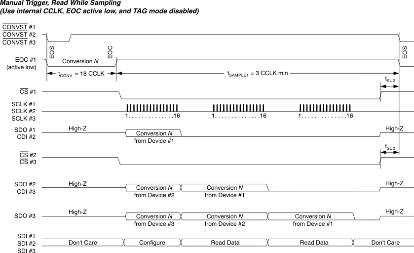 Figure 47. Simplified Dasiy-Chain Mode Timing With Shared CONVST and Continuous CS
The multiple CS signals must be handled with care when the converters are operating in daisy-chain mode. The different chip select signals must be low for the entire data transfer (in this example, 48 bits for three conversions). The first 16-bit word after the falling chip select is always the data from the chip that received the chip select signal.
Case 1: If chip select is not toggled (CS stays low), the next 16 bits of data are from the upstream converter, and so on. This configuration is shown in Figure 47.
Case 2: If the chip select is toggled during a daisy-chain mode data transfer cycle, as illustrated in Figure 48, the same data from the converter are read out again and again in all three discrete 16-bit cycles. This state is not a desired result.
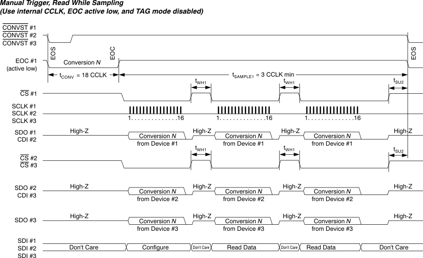 Figure 48. Simplified Daisy-Chain Mode Timing With Shared CONVST and Noncontinuous CS
Figure 49 shows a slightly different scenario where CONVST is not shared with the second converter. Converters #1 and #3 have the same CONVST signal. In this case, converter #2 simply passes previous conversion data downstream.
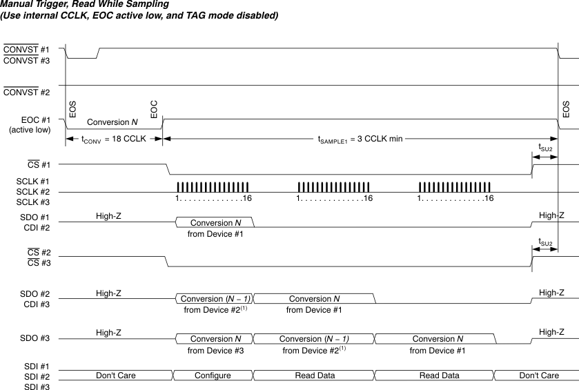
The number of SCLKs required for a serial read cycle depends on the combination of different read modes, TAG mode, daisy-chain mode, and the manner in which a channel is selected (for example, Auto Channel Select mode). The required number of SCLKs for different readout modes are listed in Table 7.
Table 7. Required SCLKs kor Different Readout Mode Combinations
| DAISY-CHAIN MODE CFR_D5 |
TAG MODE CFR_D1 |
NUMBER OF SCLK CYCLES PER SPI READ |
TRAILING BITS |
|---|---|---|---|
| 1 | 0 | 16 | None |
| 1 | 1 | ≥ 19 | TAG bits plus up to 5 zeros |
| 0 | 0 | 16 | None |
| 0 | 1 | 24 | TAG bits plus 5 zeros |
SCLK skew between converters in a daisy-chain configuration can affect the maximum frequency of SCLK. The skew can also be affected by supply voltage and loading. It may be necessary to slow down the SCLK when the devices are configured in daisy-chain mode.
9.5.5 Reset Function
The ADS833x can be reset with three different methods: internal POR, software reset, and external reset using the RESET pin.
The internal POR circuit is activated when power is initially applied to the converter. This internal circuit eliminates the need for commands to be sent to the converter after power on to set the default mode of operation (see the Power-On Sequence Timing section for further details).
Software reset can be used to place the converter in the default mode by setting the CFR_D0 bit to 0 in the Configuration register (see Table 5). This bit is automatically returned to 1 (default) after the converter is reset. This reset method is useful in systems that cannot dedicate a separate control signal to the RESET pin. In these situations, the RESET pin must be connected to VBD for the ADS833x to operate properly.
If communication in the system becomes corrupted and a software reset cannot be issued, the RESET pin can be used to reset the device manually. To reset the device and return the device to default mode, this pin must held low for a minimum of 25 ns.
After the ADS833x detects a reset condition, the minimum time before the device can be reconfigured by FS/CS going low and data clocking in on SDI is 2 μs.
