SLAS468A June   2005  – August 2016 ADS7887 , ADS7888

PRODUCTION DATA.  

  1. Features
  2. Applications
  3. Description
  4. Revision History
  5. Companion Products
  6. Device Comparison
  7. Pin Configuration and Functions
  8. Specifications
    1. 8.1 Absolute Maximum Ratings
    2. 8.2 ESD Ratings
    3. 8.3 Recommended Operating Conditions
    4. 8.4 Thermal Information
    5. 8.5 Electrical Characteristics - ADS7887
    6. 8.6 Electrical Characteristics - ADS7888
    7. 8.7 Timing Requirements
    8. 8.8 Typical Characteristics
      1. 8.8.1 ADS7887 and ADS7888
      2. 8.8.2 ADS7887 Only
      3. 8.8.3 ADS7888 Only
  9. Detailed Description
    1. 9.1 Overview
      1. 9.1.1 Driving the VIN and VDD Pins of the ADS7887 and ADS7888
    2. 9.2 Functional Block Diagram
    3. 9.3 Feature Description
      1. 9.3.1 ADS7887 Operation
      2. 9.3.2 ADS7888 Operation
    4. 9.4 Device Functional Modes
      1. 9.4.1 Power-Down Mode
  10. 10Application and Implementation
    1. 10.1 Application Information
    2. 10.2 Typical Application
      1. 10.2.1 Design Requirements
      2. 10.2.2 Detailed Design Procedure
      3. 10.2.3 Application Curves
  11. 11Power Supply Recommendations
  12. 12Layout
    1. 12.1 Layout Guidelines
    2. 12.2 Layout Example
  13. 13Device and Documentation Support
    1. 13.1 Documentation Support
      1. 13.1.1 Related Documentation
    2. 13.2 Related Links
    3. 13.3 Receiving Notification of Documentation Updates
    4. 13.4 Community Resources
    5. 13.5 Trademarks
    6. 13.6 Electrostatic Discharge Caution
    7. 13.7 Glossary
  14. 14Mechanical, Packaging, and Orderable Information

封装选项

机械数据 (封装 | 引脚)
散热焊盘机械数据 (封装 | 引脚)
订购信息

11 Power Supply Recommendations

The reference voltage for the ADS7887 and ADS7888 A/D converters are derived from the supply voltage internally. The supply to these converters must be driven with a low impedance source and must be decoupled to the ground Decouple the VDD with 1-µF ceramic decoupling capacitors, as shown in Figure 40. Always set the VDD supply to be greater than or equal to the maximum input signal to avoid saturation of codes.
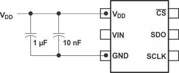
ADS7887 ADS7888 sp_ref_cap_las468.gif Figure 40. Supply and Reference Decoupling Capacitors
ADS7887 ADS7888 ref_las468.gif Figure 41. Using the REF3030 Reference
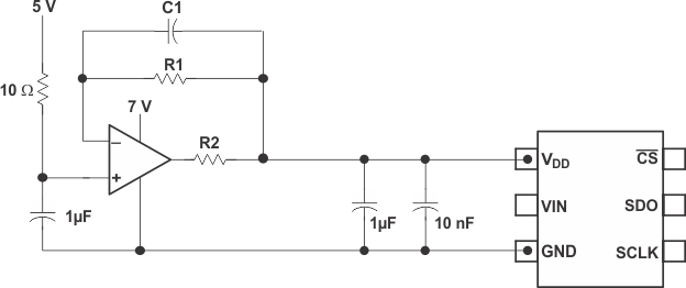
ADS7887 ADS7888 buff_las468.gif Figure 42. Buffering With the OPA735