ZHCSCB7A January 2014 – April 2014 ADS7251 , ADS7851
PRODUCTION DATA.
- 1 特性
- 2 应用范围
- 3 说明
- 4 修订历史记录
- 5 Terminal Configuration and Functions
-
6 Specifications
- 6.1 Absolute Maximum Ratings
- 6.2 Handling Ratings
- 6.3 Recommended Operating Conditions
- 6.4 Thermal Information
- 6.5 Electrical Characteristics: ADS7251
- 6.6 Electrical Characteristics: ADS7851
- 6.7 Electrical Characteristics: Common
- 6.8 ADS7251 Timing Characteristics
- 6.9 ADS7851 Timing Characteristics
- 6.10 Typical Characteristics: ADS7251
- 6.11 Typical Characteristics: ADS7851
- 6.12 Typical Characteristics: Common
- 7 Detailed Description
- 8 Application and Implementation
- 9 Power Supply Recommendations
- 10Layout
- 11器件和文档支持
- 12机械封装和可订购信息
5 Terminal Configuration and Functions
RTE Package
WQFN-16
(Top View)
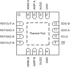
Terminal Descriptions
| TERMINAL | I/O | DESCRIPTION | |
|---|---|---|---|
| NAME | NO. | ||
| AINM-A | 16 | Analog input | Negative analog input, channel A |
| AINP-A | 15 | Analog input | Positive analog input, channel A |
| AINM-B | 5 | Analog input | Negative analog input, channel B |
| AINP-B | 6 | Analog input | Positive analog input, channel B |
| AVDD | 14 | Supply | ADC supply voltage |
| CS | 9 | Digital input | Chip-select signal; active low |
| DVDD | 7 | Supply | Digital I/O supply |
| GND | 8, 13 | Supply | Digital ground |
| REFGND-A | 2 | Supply | Reference ground potential, channel A |
| REFGND-B | 3 | Supply | Reference ground potential, channel B |
| REFOUT-A | 1 | Analog output | Reference voltage output, REF_A |
| REFOUT-B | 4 | Analog output | Reference voltage output, REF_B |
| SCLK | 10 | Digital input | Serial communication clock |
| SDO-A | 11 | Digital output | Data output for serial communication, channel A |
| SDO-B | 12 | Digital output | Data output for serial communication, channel B |
| Thermal pad | Supply | Exposed thermal pad. TI recommends connecting this pin to the printed circuit board (PCB) ground. |
|